
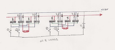
Bipolar Stepper Motor circuit
In electronic circuits, the Source and Drain pins are integral components of field-effect transistors (FETs), which are widely used in various applications including amplifiers, switches, and signal modulation. The Source pin is typically the terminal through which carriers (electrons or holes) enter the channel, while the Drain pin is where they exit. Understanding the voltage levels at these pins is crucial for proper circuit functionality.
In an n-channel MOSFET, for instance, the Source pin is connected to the ground or a lower voltage level, allowing electrons to flow from the Source to the Drain when a positive voltage is applied to the Gate pin. Conversely, in a p-channel MOSFET, the Source pin is connected to a higher voltage level, allowing holes to flow from the Source to the Drain when a negative voltage is applied to the Gate pin.
The voltage differential between the Source and Drain pins is essential for controlling the flow of current within the circuit. A proper biasing of these pins ensures that the transistor operates in the desired region—cut-off, saturation, or linear. Designers must consider the maximum voltage ratings and current capabilities of the components to avoid breakdown and ensure reliability in the circuit operation.
In summary, the relationship between the Source and Drain pins, along with their respective voltage levels, is foundational in understanding the operation of transistors within electronic circuits. This knowledge is essential for designing efficient and effective electronic systems.So I had a lot of trouble figuring out that the Source pin goes to low voltage (source of electrons) and the Drain pin goes to high voltage (absorbs electrons). Basic electricity, but it still took me a while. 🔗 External reference
Related Circuits

The circuit illustrated in FIG. 3 + 20 features SBi as the start button, SB2 as the stop button, Hi for run lights, and Hz for down lights. The subsequent circuit description aims to prevent tediousness by omitting the...

The following circuit illustrates an RF amplifier designed for FM frequencies ranging from 88 to 108 MHz with a broadband configuration. This circuit utilizes the BLV10 transistor. The RF amplifier circuit operates within the FM broadcast band, which is crucial...
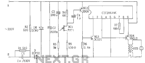
The rice cooker notification circuit operates as follows: When the rice cooker is in operation, both terminals A and B have a voltage of 0, meaning the entire circuit remains inactive. In the event that the rice cooker runs...

The LED flasher circuits below operate on a single 1.5 volt battery. The circuit on the upper right uses the popular LM3909 LED flasher IC and requires only a timing capacitor and LED. The top left circuit, designed by...

The popularity and easy access of RS-232 ports lend them to many communication projects. You can use a port as is or as a tiny parallel port when the exchange uses only control lines. Before the asynchronous serial-data transfer...

A common diode balanced modulator circuit is illustrated. It comprises two identical performance diodes and a center-tapped transformer configuration. The diodes used are VD1 and VD2, specifically 2AP9 models. The parameters for the circuit elements are detailed in FIG....