
FM PLL transmitter
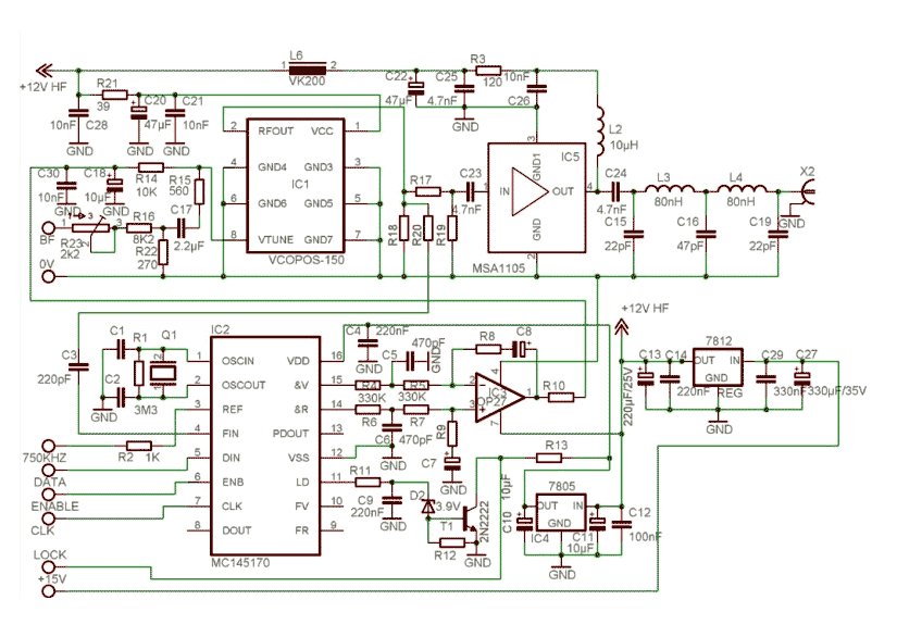
The FM transmitter circuit utilizes the POS150 integrated voltage-controlled oscillator (VCO) from Mini-Circuits, which is designed to operate across the entire FM band, specifically from 87.5 MHz to 108 MHz. The VCO operates within a voltage range of 4V to 8V, providing a stable frequency output with a Kvco factor that remains consistent across the FM spectrum. This stability allows for direct application of the audio frequency (AF) signal onto the control voltage line connected to the phase-locked loop (PLL), facilitating efficient modulation without the need for RF tuning.
An essential component of this design is a 4dB attenuator, which is strategically placed to prevent the VCO from exceeding the 1dB gain compression point when interfacing with the MSA1105 RF power stage. This careful design consideration ensures that the transmitter maintains optimal performance without distortion or signal degradation.
To further enhance performance, a low-pass filter is integrated into the output stage of the circuit. This filter effectively reduces harmonic emissions, achieving a harmonic rejection of -60 dBc, which is critical for compliance with regulatory standards and to minimize interference with adjacent channels. The transmitter is designed to exhibit a phase noise of -103 dBc/Hz at a 10 kHz offset from the carrier frequency, indicating high spectral purity.
The transmitter's output power is rated at 50 mW (+17 dBm), making it suitable for short-range transmission applications. The modulation scheme employed is direct frequency modulation, which allows for efficient encoding of audio signals. The MPX input response is specified to maintain a tolerance of +/-0.5 dB across a frequency range of 30 Hz to 60 kHz, ensuring high fidelity in audio reproduction. The minimum input level for the MPX is set at 300 mV RMS, which is adequate for most audio sources.
Power supply requirements for this FM transmitter range from 14V to 18V, providing the necessary headroom for the VCO and RF power stage to operate effectively. The frequency stability is maintained within +/- 400 Hz, ensuring reliable performance across varying environmental conditions. The design also includes specifications for spurious emissions, which are limited to below -70 dBc, further enhancing the overall quality of the transmitted signal.This new FM transmitter is very easy to make and doesn't need any RF tuning. First of all ,we have used an integrated VCO: The POS150 from Mini-circuits. This excellent RF circuit covers all the FM Band in a voltage range of 4V to 8V. The Kvco factor is very stable all over the FM band, consequently, we have applied the AF signal directly on the control voltage line coming from the PLL. A 4dB attenuator allows the VCO to drive the MSA1105 RF power stage without exceeding the 1dB gain compression.
Finally,a low pass filter ensures a good harmonics rejection.(H3<-60dBc). This new design conducts to new RF performances like: Phase/noise equals to -103dBc/Hz at 10KHz from the carrier.. +17dBm output power level (50mW). Power Output=50mW. Frequency Output=87.5MHz to 108 MHz. Frequency Step=10KHz. Phase Noise=-103dBc/Hz. Frequency Stability= +/- 400Hz. Harmonic Filtering=<-60dBc. Spurious Emissions= <-70dBc Modulation=Direct Frequency Modulation. MPX Input Response=+/-0.5dB 30Hz to 60KHz. MPX Input Level =300mV RMS Min. Power Supply=14 to18V. 🔗 External reference
Related Circuits
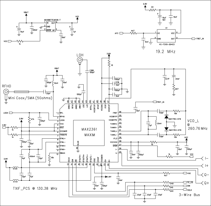
This application note outlines the use of the MAX2361 quadrature transmitter integrated circuit (IC) within the Korean Personal Communications Service (PCS) band, specifically for transmission frequencies ranging from 1750 to 1780 MHz. The MAX2361 is a high-performance quadrature transmitter designed...
The FM302E-I-type FM transmitter exciter is utilized in Japan's NEC HPB a 1210 motherboard. It features direct carrier frequency modulation, phase-locked frequency stabilization, and frequency synthesis. The preamplifier (BLF-177 FET) is directly driven by an actuator, achieving a maximum...
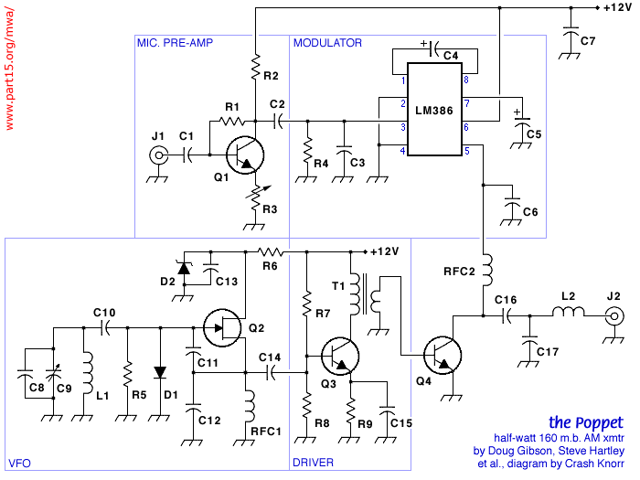
The Poppet is a half-watt AM transmitter designed by Mr. Doug Gibson of England. The original design was published in issue 84 of SPRAT, the newsletter of the GQRP Club. The version presented here incorporates modifications suggested by Steve...
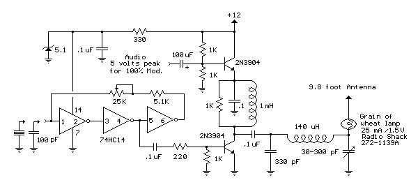
In this circuit, a 74HC14 hex Schmitt trigger inverter is used as a square wave oscillator to drive a small signal transistor in a class C amplifier configuration. The oscillator frequency can be either fixed by a crystal or...
Instead of concentrating on the mathematical and theoretical aspects of this simple pyro RF transmitter, the focus will be on the components within each stage. The mathematics involved in understanding how and why this circuit operates is complex and...
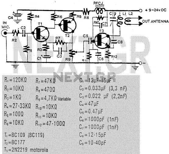
This is a nice 2 Watts FM transmitter. It has a Super-Sensitive pre-amplification with BC109 and BC177 with more than 100% signal modulation. The job finish the 2N2219 by Motorola. For the Coils you should use 1mm wire(enameled), L1=...