
For driving the power supply circuit of the sensor bridge
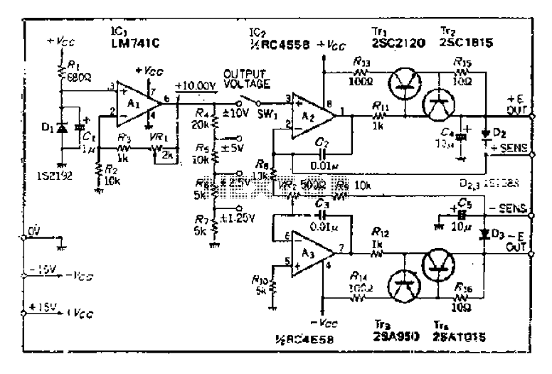
The circuit design features a maximum input voltage specification of 10V, which is critical for ensuring the safety and functionality of the operational amplifier (op-amp) employed in the circuit. The reference voltage of 10V is generated through the op-amp, which operates in conjunction with a temperature-compensated Zener diode (IS2192). The Zener diode is selected for its stability across varying temperatures, which is essential for maintaining a consistent output voltage.
The Zener voltage (Vz) can be fine-tuned via a variable resistor, allowing for precise adjustments to counteract any discrepancies that may arise during operation. This variable resistor is crucial for calibrating the circuit to achieve the desired performance specifications. A resistor divider circuit, consisting of resistors R4 and R1, is implemented to facilitate the switching of input voltage levels to the op-amp. This configuration is designed to provide a descending order of input voltages, which can be beneficial for applications requiring varying voltage levels.
To ensure sustained voltage accuracy over time, it is imperative to select resistances that exhibit minimal variation. The recommended range for these resistances is between 0.5 to 10 ohms, which helps to mitigate the effects of drift and enhances the reliability of the circuit.
The circuit incorporates an op-amp buffer amplifier with a gain of 1, which serves to isolate the input from the output, thereby preventing loading effects that could compromise performance. The buffer amplifier is configured positively, ensuring that the output voltage remains in phase with the input voltage. Furthermore, an inverting amplifier configuration is employed to produce a negative voltage output from the circuit. This is achieved by utilizing feedback through a resistor network, which allows for the inversion of the output voltage while maintaining accuracy.
To address potential resistance errors, a variable resistor is included in the design. This component allows for real-time adjustments, facilitating the correction of any inaccuracies in the voltage output. The implementation of these design elements collectively ensures that the circuit operates efficiently, providing stable and precise voltage references as required for various electronic applications.A. The maximum input voltage of 10V. OP amplifier A, to give ten of 10V reference voltage, and its stability is mainly determined by the Zener diode characteristics, mining com mission temperature compensated zener diode (IS2192). Zener voltage Vz if the error can be used to adjust the variable resistor, it is IO. oov. s resistor divider circuit (R4vR,) to switch A, input voltage, ul/2 office units in descending order. When you need to 1 voltage accuracy over time, EU resistance must choose a small difference in disrespect of the product ( 0.5 ~ .10 {).
OP/Ze buffer amplifier 4. The amplifier, save magnification is 1, is positive to put large, but with sleep} line inverting amplifier, the output voltage into a negative voltage inverter output voltage. - said that the resistance r, four errors on a variable resistor r z mouth into line correction, accurate voltage can be obtained.
Related Circuits
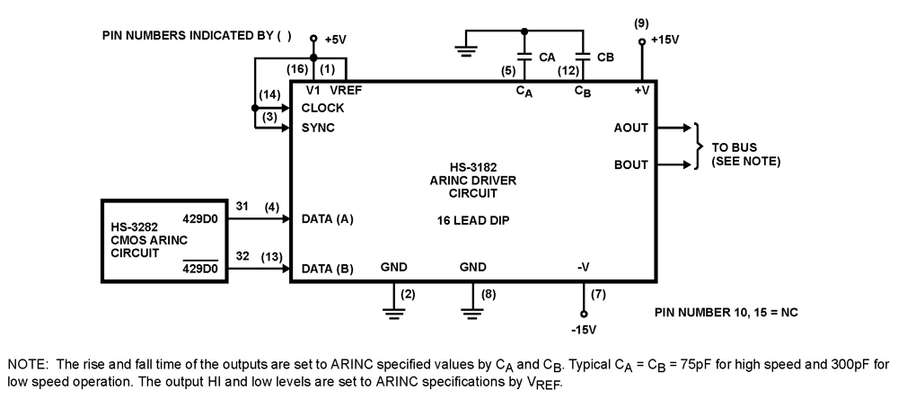
The HS-3182 is a monolithic dielectrically isolated bipolar differential line driver designed to meet the specifications of ARINC 429. This device is intended to be used with a companion chip, the HS-3282 CMOS ARINC Bus Interface Circuit, which provides...
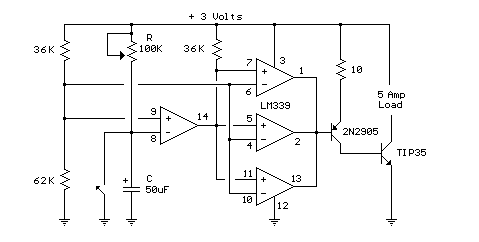
This circuit utilizes an LM339 quad voltage comparator to create a time delay and manage a high current output at low voltage levels. Approximately 5 amps of current can be sourced using a pair of fresh alkaline D batteries....
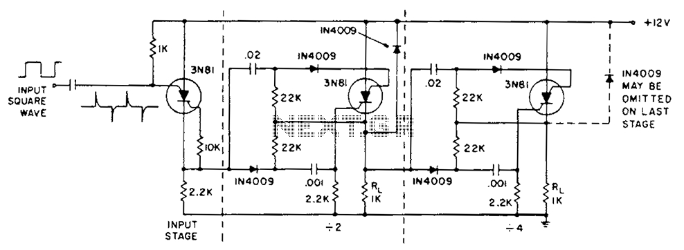
The circuit operation is initiated by a positive edge signal. The anodes of the triac switches are activated while the cathodes of the switches remain closed. A male-female IN4009 diode is utilized for positive transient suppression, ensuring that the...

The phase and neutral wires from the power source have already been connected to electrical appliances such as fans and light points. According to the UPS connection diagram, an additional phase wire should be connected to those appliances where...
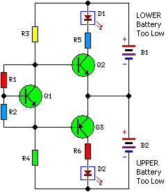
Most 24V power systems in trucks, 4WDs, RVs, boats, and similar applications utilize two series-connected 12V lead-acid batteries. The charging system is designed to maintain the total voltage of the two batteries. If one battery begins to fail, the...
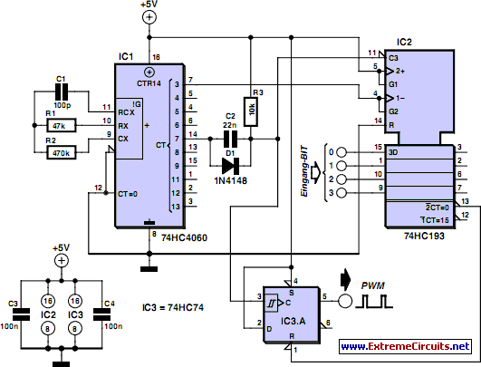
PWM waveforms are frequently employed to regulate the speed of DC motors. The mark/space ratio of the digital waveform can be established either by utilizing an adjustable analog voltage level (as seen in a NE555-based PWM generator) or through...
Warning: include(partials/cookie-banner.php): Failed to open stream: Permission denied in /var/www/html/nextgr/view-circuit.php on line 713
Warning: include(): Failed opening 'partials/cookie-banner.php' for inclusion (include_path='.:/usr/share/php') in /var/www/html/nextgr/view-circuit.php on line 713