
Four-Trace Oscilloscope Adapter
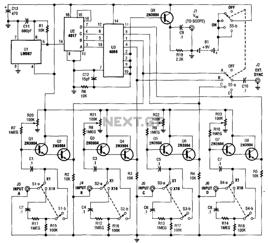
The described circuit functions as a versatile adapter designed to enhance the functionality of basic oscilloscopes by enabling four-trace operation. The core of the circuit is an oscillator, specifically a 567 phase-locked loop (PLL), which generates a stable frequency signal to drive the subsequent counter (U2). This counter is responsible for sequentially selecting one of the four available scope preamplifiers (Q1/Q2 through Q7/Q8), allowing for the observation of multiple signals on a single oscilloscope display.
The output from the selected preamplifier is then sent to a buffer stage (Q9) to ensure that the signal integrity is maintained before being routed to output jack J1. This output jack serves as the primary connection point for the oscilloscope, allowing for easy signal monitoring. Additionally, output jack J2 is dedicated to providing synchronization signals to the oscilloscope, ensuring that the displayed waveforms are properly aligned and timed.
Resistors R20 through R23 act as posting controls for channels A through D (connected to jacks J3 through J6), allowing for fine adjustments of the signal levels being fed into the oscilloscope. This feature is particularly useful for optimizing the display of different signal amplitudes, ensuring that the user can accurately analyze the characteristics of each signal.
The circuit incorporates switched attenuators (S1A-B through S4A-B) for each channel, enabling the user to adjust the signal attenuation as needed. This flexibility is essential for accommodating a wide range of input signal levels, from 0 to 20 V, making the adapter suitable for various applications. The switching rate of approximately 125 kHz allows for rapid channel selection, ensuring that the user can quickly switch between different signals without noticeable delay.
Overall, this simple adapter circuit significantly enhances the capabilities of low-cost oscilloscopes, transforming them into powerful tools for multi-channel signal analysis. The careful integration of oscillators, counters, buffers, and attenuators facilitates a user-friendly experience while maintaining high signal fidelity and operational efficiency. This simple adapter uses an oscillator (567) to drive a counter (U2) and switch (U3) that selects the outpu t of one of four scope preamps (Q1/Q2 through Q7/Q8) and feeds it to buffer Q9 and output jack Jl. J2 provides synch to the scope. R20 through R23 are posting controls for channels A through D (J3 through J6). SlA-B through S4A-B are switched attenuators, one for each channel. Switching rate is about 125 kHz. This circuit is useful for adding four-trace operation to inexpensive oscilloscopes. Signal levels of 0 to 20 V can be handled. 🔗 External reference
Related Circuits
This simple circuit allows the use of an oscilloscope as a Time Domain Reflectometer (TDR). The operation involves sending a pulse down a cable and observing the resulting reflections. The circuit design for utilizing an oscilloscope as a Time Domain...
The input attenuator uses a commutating capacitor to cancel the input capacitance of the FET buffer (see DC-10 MHz amp schematic). The commutating capacitors are absolutely necessary to cancel the effect of the input capacitance to the DC-10MHz amplifier....
Whenever I'm in the car listening to my favourite CD, it always happens - my batteries go dead. To solve that problem, I built this extremely simple regulator circuit. It steps down the 12V from the lighter socket to...
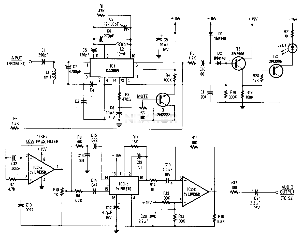
The baseband audio input originates from the pole of switch S1 in the stereo decoder and is coupled to IC1 (a CA3089) via a 78.6 kHz bandpass filter composed of capacitors C1 and C2, along with inductor L1. IC1...
This circuit allows for the simultaneous display of four signals using a single channel of an oscilloscope. It sequentially switches each input to the output with some signal processing in between. It is designed for low-frequency signal measurements and...
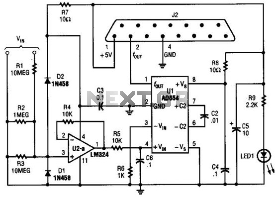
The adapter comprises a voltage-to-frequency converter integrated with a signal conditioning and protection circuit. J2 interfaces with the game port of a personal computer. Additional software references are available for use with this circuit. The voltage-to-frequency adapter functions by converting...