
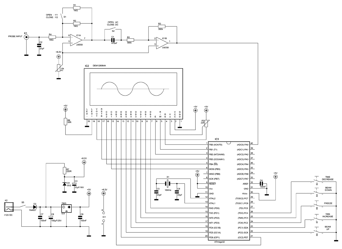
Four-Channel Oscilloscope Adaptor
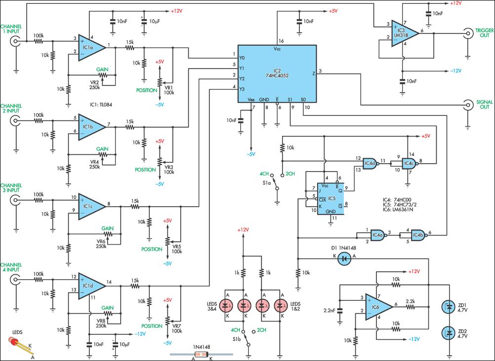
The circuit is structured around a robust design that facilitates the simultaneous observation of multiple signals without the need for multiple oscilloscope channels. Each input is processed through the TL084 op-amp, which is known for its low noise and high precision, making it ideal for sensitive signal measurements. The attenuation stage preceding the op-amp ensures that higher voltage signals are brought within the acceptable range for processing, thereby protecting the circuit from potential damage while maintaining signal integrity.
The gain adjustment feature provided by VR2 allows for precise calibration, ensuring that the displayed signal accurately reflects the input voltage levels. This is particularly useful in applications where signal amplitudes may vary significantly. The addition of a DC offset via VR1 enhances the versatility of the circuit, allowing users to manipulate the vertical positioning of the traces on the oscilloscope display for clearer differentiation.
The use of a 4-channel multiplexer (IC2) is a critical component in the design, enabling the selection of different signal paths based on the control signals generated by the oscillator circuit. The oscillator's frequency and the subsequent signal cleaning stages ensure that the multiplexer receives clean, well-defined signals, which are crucial for accurate representation on the oscilloscope.
The triggering mechanism is essential for synchronizing the oscilloscope display with the rapidly switching signals. By utilizing a dedicated buffer circuit, the design ensures that the oscilloscope can reliably capture and display the signals, even as they switch at high speeds. This thoughtful integration of components results in a sophisticated yet user-friendly circuit capable of handling a variety of low-frequency signal measurement tasks efficiently.This circuit enables you to display four signals simultaneously using only one channel of your oscilloscope. Essentially, it switches each of the inputs through to the output in turn, with some signal massaging in between.
As shown, it is suitable only for low-frequency signal measurement and does not include over-voltage protection at the inputs. Each input circuit is identical, utilising one amplifier from a TL084 quad op amp package. Looking at channel 1, the input signal is attenuated by a factor of 10 by the 100k © and 10k © resistors before arriving at the non-inverting input of IC1a. A 15k © resistor in series with the op amp output along with a 10k © resistor to ground provide additional attenuation.
Vertical (voltage axis) adjustment is made with VR2, which sets the gain of the amplifier. This is used to calibrate or scale the displayed signal against the actual input voltage level. Using the values shown, the gain can be adjusted from unity to about a factor of 26. Note that the output of the op amp must be limited to ± 10V so that the voltage into the 4-channel multiplexer (IC2) does not exceed ± 5V. Therefore, with a gain of unity, the input voltage can range from ± 100V, whereas with a gain of 26, it must not exceed about ± 3.
85V. VR1 applies a positive or negative DC offset to the output of the op amp. This can be used to compensate for op amp input offset voltage. It can also be used to shift the vertical position of the trace on-screen to provide multiple trace separation. Note, however, that any offset will consume part of the available output swing and therefore limit signal measurement "headroom".
Each op amp output is connected to IC2, a 4-channel analog multiplexer. The logic levels on "S0" & "S1" (pins 9 & 10) determine which input channel is connected to the "Z" output (pin 3). A square wave oscillator and divider circuit are used to toggle the "S0" and "S1" pins in sequence to first select channel 1 briefly, then channel 2 and so on.
An LM6361 high-speed op amp (IC6) forms the heart of the oscillator. It operates at about 20kHz. Back-to-back zener diodes at the output clip the voltage to TTL levels, after which diode D1 passes the positive half-cycle to the input of one gate of a 74HC00 quad NAND device. IC4a & IC4b "clean up" the signal before if is applied to the S0 input of IC2. A 74HC73 J-K flip-flip (IC5) divides the oscillator frequency by two. This is used to drive the "S1" input when in 4-channel mode. In 2-channel mode (switch S1 closed), one input (pin 12) of IC4d is pulled low, which effectively holds the "S1" input permanently low.
Finally, a separate buffer circuit (IC3) is used to provide a trigger signal for the oscilloscope. This is needed because it would be difficult to trigger reliably on the main output as it switches rapidly between the four signal sources. 🔗 External reference
Related Circuits
The Xminilab-B oscilloscope is based on the Atmel AVR ATXMEGA32A4 microcontroller. It is designed as a debug board by the Gabotronis company, as noted on rlocman.ru. The Xminilab-B oscilloscope features a compact and efficient design that leverages the capabilities of...
This four-channel mixer amplifier is designed to ensure a good signal-to-noise ratio by controlling the signal levels after amplification and mixing them to produce a combined output. It is compatible with dynamic microphones ranging from 50 ohms to 50...
This is a straightforward X-Y oscilloscope design utilizing an ATmega324P microcontroller and two KAD0820 analog-to-digital converters (similar to National Semiconductor's ADC0820). The initial version of this oscilloscope was based on an AT90S4414, necessitating the use of external ADCs. Various...
A few months ago as I was surfing on the net, I saw an oscilloscope based on PIC18F2550 microcontroller and a KS0108 controller based graphical LCD. That was Steven Cholewiak's web site. I had never seen before so amazing...
The project involves the design of a custom multiplexer for a four-channel oscilloscope, allowing for simultaneous display of multiple figures with distinct X/Y inputs. The instrument is intended to enhance the functionality of existing oscilloscopes, particularly in conjunction with...
Video signals can be challenging to display on an oscilloscope. Standard trigger circuits in most oscilloscopes often struggle to achieve a stable trigger from the combined vertical and horizontal sync signals, color burst, and picture signal found in a...