
MFOS Micro-Sample & Hold circuit
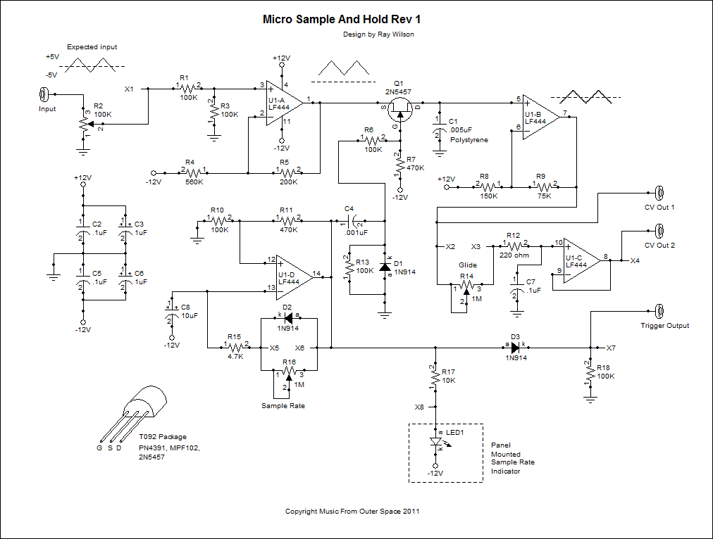
The circuit described encompasses a sample and hold system, which is critical in analog-to-digital conversion processes. The use of a potentiometer (R2) allows for the adjustment of input voltage levels, ensuring compatibility with the operational amplifier (U1-A) and preventing clipping by the JFET (Q1). The voltage divider formed by R1 and R3 is essential for scaling the signal appropriately before amplification and level shifting, which is crucial for maintaining signal integrity.
The JFET (Q1) operates as a switch, controlled by the sample clock pulses generated by U1-D, allowing precise timing in capturing the input signal's voltage. The capacitor (C1) serves as the storage element for the sampled voltage, which is buffered by U1-B to maintain signal fidelity over time. The LF444 op-amp's low input current characteristic is advantageous for minimizing leakage and ensuring that the sampled voltage remains stable during the hold phase.
The sample clock generator (U1-D) is integral to the operation of the sample and hold circuit, providing the necessary timing signals to control the sampling process. The asymmetric rectangular wave output ensures that the capacitor can charge efficiently while allowing for adjustable sample rates, accommodating various application requirements. The overall design emphasizes precision in sampling and holding voltages, which is fundamental for accurate signal processing in electronic systems.Voltage to be sampled is applied to the input which is one end of R2 (100K linear taper potentiometer). The other end of R2 is grounded and thus the level of signal applied to buffering level shifter U1-A and associated components is controlled by R2.
Signals applied to the sample and hold (at point X1) can oscillate about ground but should not exceed about +/-5. 5 volts. That is why the design was changed to allow for higher level signals since they can be attenuated by adjusting R2. If the voltage at pin 1 of U1-A goes below ground Q1 can clip the signal and improper sampling results.
R1 and R3 comprise a voltage divider which causes the applied attenuated signal to be effectively cut down to half of it`s level. This signal is applied to U1-A (1/4 LF444 quad op amp) where it is level shifted and given a gain of about 1.
5. Here you can see the comparison of the input signal to the signal at pin 1 of U1-A. Q1 N-Channel JFET 2N5457 acts like a closed switch (between source and drain) when it`s gate is brought slightly above ground by differentiated pulses which are generated by picking off the front end of the rectangle wave output by U1-D sample clock generator. Normally (when no pulse is being applied) the gate of Q1 is held at about -3. 6V by resistor network R7, R6 and R13. The voltage that is present at the source of Q1 passes through to the drain and charges (or discharges as the case may be) C1 where the sampled voltage is held until the next pulse hits the gate.
U1-B buffers the sample held on the cap. The LF444CN chip has ultra low input current which allows the sample to sit on the cap and be buffered by U1-B for quite some time. With no pulse applied to the gate of Q1 it essentially acts like an open switch (source to drain) and the voltage on C1 does not leak back through the transistor.
Buffer U1-B applies gain of about 1. 5 and also level shifts the signal so that it approximates the original input level and oscillates about ground. This is the sampled and held voltage (blue) as it compares to the input voltage (yellow). Notice the level is shfted so that it reflects the actual input signal level. This is the differentiated pulse that is applied to the gate of Q1 via C4 in series with R6. Q1 source to drain is essentially a closed switch during the pulse. The output changes during the pulse as a new sample is acquired. Sample clock generator U1-D and associated components works as follows. If we begin our analysis imagining that the output of U1-D just went low (to about -11V) we see that the voltage level applied to U1-D pin 12 is about -1.
9 volts. C8 (10uF aluminum or tantalum electrolytic capacitor) which had previously been charged (remember U1-D just went low and was high prior to that transition) to well above ground (actually to about 2V) begins to discharge via R15 and 1M Sample Rate adjust pot R16. When C8 discharges to below -1. 9 volts (the level on pin 12 remember) the output of U1-D shoots to about +11V causing the voltage at U1-D pin 12 to go to about +1.
9V and also causing C8 to charge from it`s previous voltage (about -2V) towards V+ via D2 (1N914 high speed diode) and R15 (4. 7K resistor). When C8 charges to above the level on U1-D pin 12 (about +2V), U1-D`s output shots low again and this cycle continues.
The output of U1-D is an asymmetric rectangular pulse wave due to D2 which allows the positive excursion of U1-D to charge C8 without the effect of 1M Sample Rate pot R16. Thus the high time is limited to about 20 mS and the low time depends on the setting of 1M Sample Rate pot R16.
The rate of the sample clock can be varied from about 0. 33 hertz to about 30 hertz. The sample clock`s output is fed through D3 (1N914) and dropped on R18 (100K resistor) and then connected to the jack for the trigger output. These are the signals observed on the inputs of U1-D. The blue waveform is the charge and discharge of C8 on U1-D pin 13. The 🔗 External reference
Related Circuits
This is a request for assistance in designing a circuit for a tape delay unit. The mechanical components are functioning well, but the circuit integration remains a challenge. The tape heads used are cassette tape heads with a resistance...
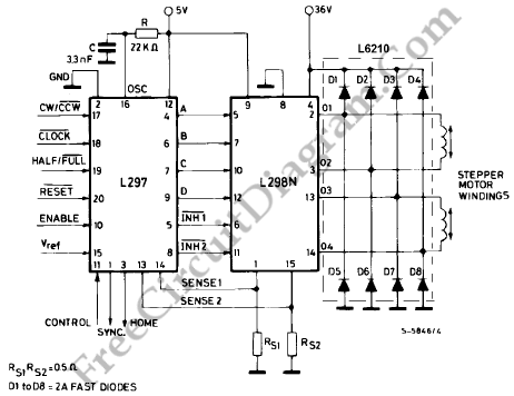
The L29 Stepper Motor Controller IC facilitates the control of four drive signals for two bipolar and four unipolar footfall motors in a microcomputer-controlled appliance. It allows for motor operation in half-step, full-step, and wave drive modes, utilizing switch-mode...
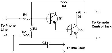
This compact circuit enables automatic recording of phone conversations. It connects to the phone line, the microphone input of a tape recorder, and the remote control jack of the recorder. The circuit detects the voltage level in the phone...
Circuit audio peak indicator circuit schematics. Circuit Electronics, schematics for audio peak indicator circuit. An audio peak indicator circuit is designed to visually represent the peak levels of an audio signal, providing critical information for audio engineers and musicians regarding...

This simple circuit can be used to sense the distance between the rear bumper of a car and any obstacle behind it. The distance is indicated by the combination of LEDs (D5 to D7) that illuminate: at 25 cm,...
Schematic and description of a simple and easy-to-build NiCd and NiMH battery charger circuit that is capable of charging multiple NiCd and NiMH batteries. The circuit for the NiCd and NiMH battery charger is designed to be straightforward, allowing for...
Warning: include(partials/cookie-banner.php): Failed to open stream: Permission denied in /var/www/html/nextgr/view-circuit.php on line 713
Warning: include(): Failed opening 'partials/cookie-banner.php' for inclusion (include_path='.:/usr/share/php') in /var/www/html/nextgr/view-circuit.php on line 713