
Frequency Divider
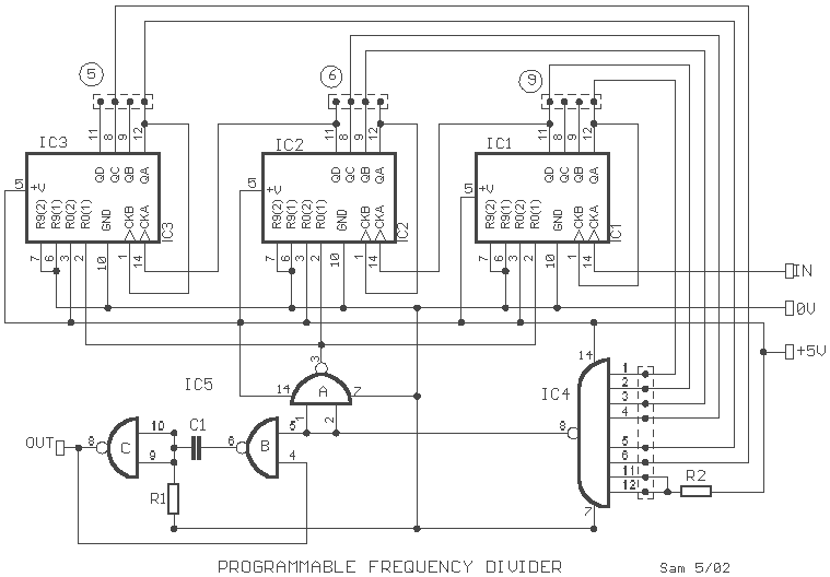
The described frequency divider circuit utilizes three 7490 decade counters (IC1, IC2, and IC3) configured in a cascading arrangement to achieve a division ratio of up to 999. Each 7490 counter is capable of counting from 0 to 9, and when cascaded, they effectively form a binary coded decimal (BCD) counter. The input signal, a TTL compatible square wave, is fed into the first counter (IC1), which increments its count with each pulse. As the count progresses through the three counters, the total count is represented in BCD format.
Once the cumulative count reaches the predetermined division ratio, all outputs of the fourth integrated circuit (IC4), which is a 7430 NAND gate, will transition to a high state. This state change causes the output of IC4 to drop low, which serves as a trigger for the monostable multivibrator formed by IC5B and IC5C. The output pulse generated by this monostable multivibrator is short, effectively resetting the counters by driving the output of IC5A high. This reset allows the counting process to restart, enabling continuous frequency division.
To program the circuit for a specific division ratio, the BCD equivalent of the desired ratio must be calculated and set on the inputs of the counters. For instance, a division ratio of 569 would require the BCD representation of 5 (0101), 6 (0110), and 9 (1001) to be applied to the corresponding inputs of the counters. It is important to note that not all division ratios are feasible; for example, a division ratio of 777 cannot be achieved with this configuration due to the limitation of only having 8 inputs available for IC4.
The circuit also includes passive components such as a 680-ohm resistor (R1) and a 100 pF ceramic capacitor (C1) for timing and stability purposes, along with a 1 kΩ resistor connected to the unused inputs of IC4 to pull them to a high state (5V). This ensures that the circuit operates correctly within the specified voltage levels for TTL logic.This circuit will divide the frequency of a TTL compatible square wave signal by a factor from 0 to 999. The circuit comprises three decade counters IC1 to IC3 and a few NAND gates. The three 7490?s are cascaded and count is the input signal. When the desired and count reached all the inputs of IC4 become high, so the output goes low. This triggers the monostable consisting of IC5B and IC5C, which provides a sort output pulse. The output of IC5A goes high, resetting the three counters and the count then begins again. To program the counter it is first necessary to work out the binary coded decimal (BCD) equivalent of the required division ratio.
In the example shown the division ratio is 569. The unused inputs of IC4 are connected to +5V via a 1K resistor. Note that the circuit will not divide by 777, since this would require 9 inputs to IC4 and only 8 are available. R1=680 ohms C1=100pF ceramic IC4=7430 R2=1 Kohms IC1-2-3=7490 IC5=7400 🔗 External reference
Related Circuits
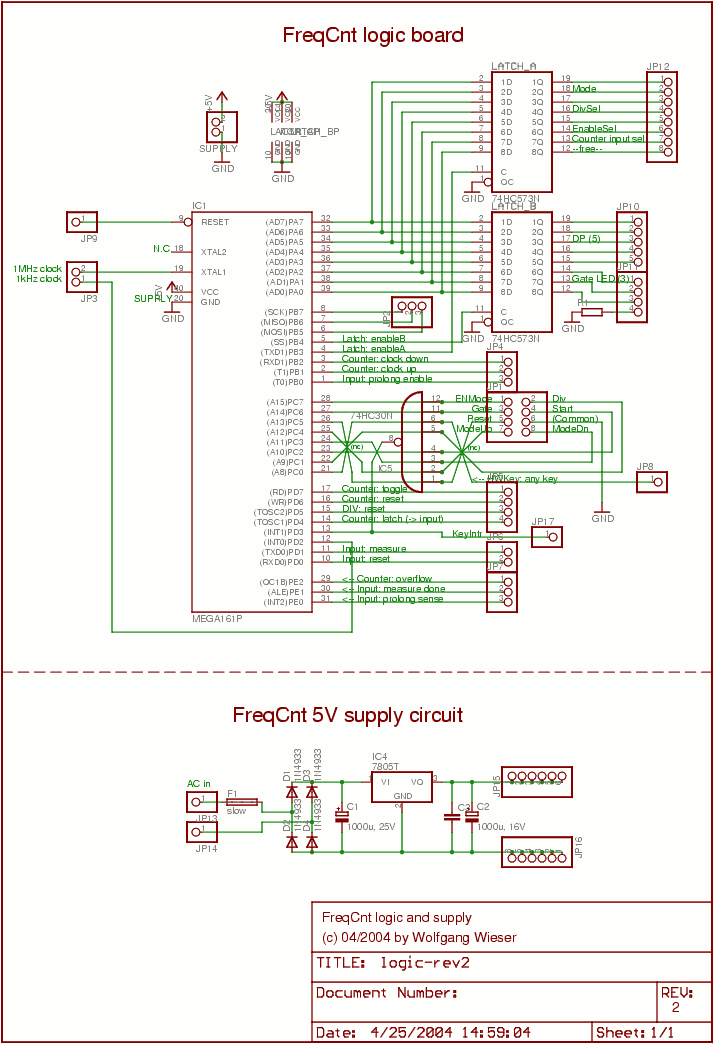
The lower schematic represents a standard bidirectional rectifier along with capacitors and a 7805 voltage regulator, which provides a stable 5V source to power the electronic components of the frequency counter. A fuse is included for security purposes. The...
The pulse repetition rate is largely unaffected by temperature and power supply voltage, and it varies linearly with V1N, the modulating voltage. Effective information transfer was achieved at distances of 12 feet (~4m) in free air. A greater range...
The crystal oscillator utilizes two sections of IC1, a 4001 quad 2-input NOR gate, representing a standard and reliable design. The oscillator generates a 1.85-MHz square-wave output that feeds into IC2, a 4017 divide-by-10 counter. The count enable and...
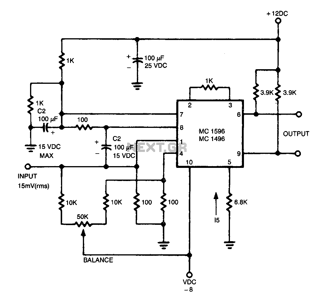
The output contains the sum component, which is twice the frequency of the input, since both input signals are of the same frequency. In a circuit design context, the described output suggests the presence of a frequency doubling mechanism, commonly...
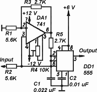
The timer is utilized in a conventional setup, with the exception that the timing resistor has been substituted with a current source derived from the operational amplifier DA1 (741). This modification enables the achievement of excellent linearity, exceeding 3%....
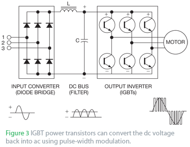
An AC drive controls AC induction motors and, similar to its DC counterparts, regulates speed, torque, and horsepower. A DC drive typically manages a shunt-wound DC motor, which features separate armature and field circuits. This teardown of the Schneider...