
Frequency Doubler
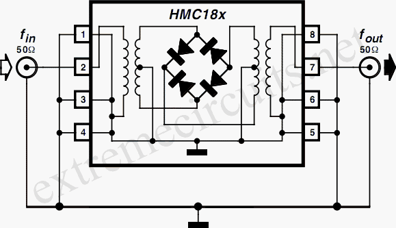
The HMC 187, HMC 188, and HMC 189 frequency doublers are designed for high-frequency applications, making them ideal for telecommunications and RF systems. The devices utilize advanced semiconductor technology to achieve high performance in terms of frequency multiplication and isolation. The passive doubler circuit architecture, incorporating Schottky diodes, ensures minimal signal distortion and high efficiency.
The baluns integrated within these devices serve to convert the balanced input signal to an unbalanced output signal, facilitating compatibility with various RF components. This matching capability is crucial for maintaining signal integrity and minimizing reflections in the circuit. The compact footprint of the HMC18x series allows for integration into space-constrained applications, making them suitable for portable and embedded systems.
The specified isolation performance of 35 dB is particularly advantageous in multi-stage applications where multiple doublers are cascaded. In such configurations, the reduced harmonic content at the output helps to simplify the design of subsequent stages, potentially eliminating the need for complex filtering solutions.
Additionally, the devices are optimized for 50 Ohm systems, which is a standard impedance in RF applications. The recommended input signal level of +15 dBm is tailored to ensure optimal performance and output power, which is critical for maintaining the desired signal levels in communication systems.
Overall, the HMC 187, HMC 188, and HMC 189 frequency doublers are versatile components that provide efficient frequency multiplication with excellent isolation, making them valuable in modern RF and microwave circuit designs.If you are working at frequencies of the order of 850MHz to 4GHz andnd that a frequency multiplier is required, the HMC 187, HMC 188 and HMC 189 (see table) frequency doubler may be just the solution you are looking for. The isolation performance of these devices ensures that the input frequency (fin) and its harmonics 3fin and 4fin are attenu
ated by 35dB relative to the wanted output frequency 2fin. This excellent isolation specification reduces the need for additional output filtering and is also an advantage where several doublers are connected in series to produce four or eight times the input frequency. The tiny outline of the HMC18x- series device occupies a board area of 3mm by 4. 8mm and measures just 1. 07 mm high. Internally the device contains balanced to unbalanced transformers (baluns) to match the doubler circuit with the output and input.
The doubler circuit itself is passive and comprises a full wave Schottky diode bridge rectifier. The monolithic baluns which are integrated on-chip give the device a relatively high low-frequency roll-off at 850MHz. Lower frequencies can also be multiplied but the conversion loss factor (given as typically 15 dB) will increase.
The input and output are matched for 50 Ohm operation and the input signal level should be of the order of +15dBm which will give a output level of approximately 0dBm. The main characteristics of the three versions of this device are summarized in the table above. 🔗 External reference
Related Circuits
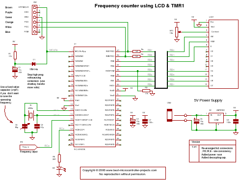
C code for a PIC frequency counter operating up to approximately 50 MHz. The project utilizes an HD47880 LCD for display purposes and employs Timer 1 to count the edges of the input signal. This frequency counter project is designed...
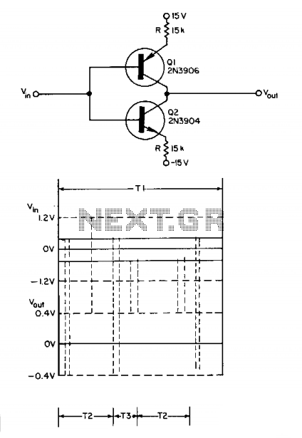
The turn-on and turn-off characteristics of two complementary transistors can be combined to achieve nonselective frequency tripling. The resulting circuit processes any periodic waveform with non-vertical edges. Each peak of the input signal generates three output signal peaks. The...
The input signal is applied to a gate G and then to a counter for a precise period of time. After this period, the input signal is stopped for a while, and then the cycle is repeated. During the...

Frequency measurement is crucial in radio construction, as it allows for the setting of desired frequencies in both receivers and transmitters, as well as monitoring frequency drifts. A frequency counter can verify oscillator functionality and ensure stability in generation....
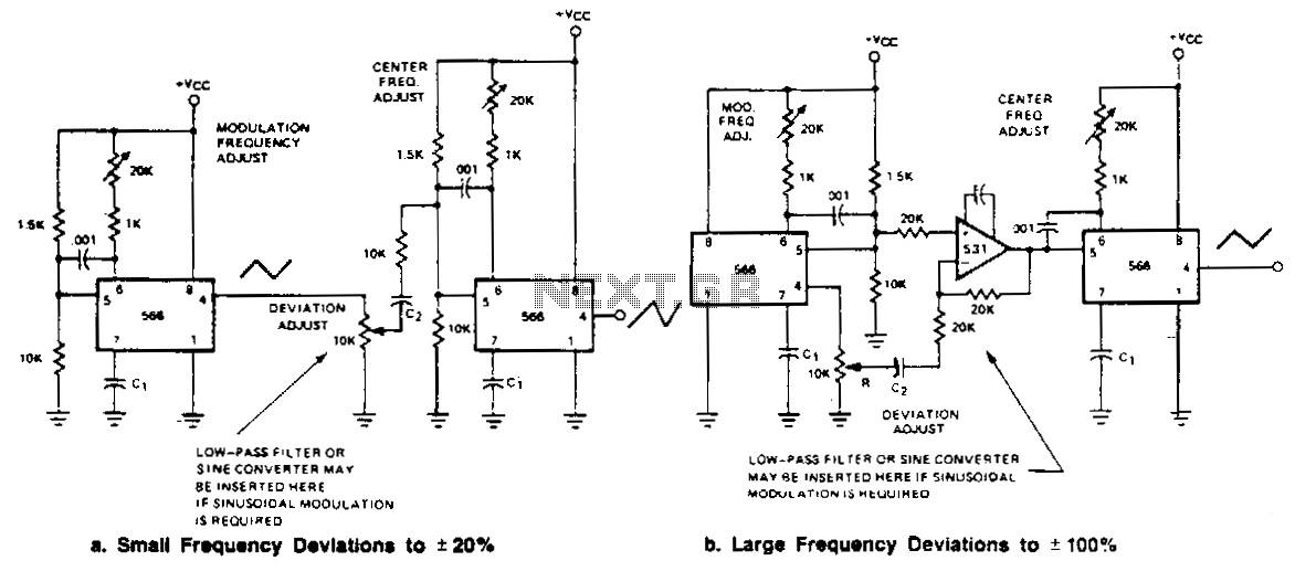
Two FM generators are presented for low frequency applications with a center frequency of less than 0.5 MHz. Each generator utilizes a 566 function generator as a modulation generator and a second 566 as the carrier generator. Capacitor C1...
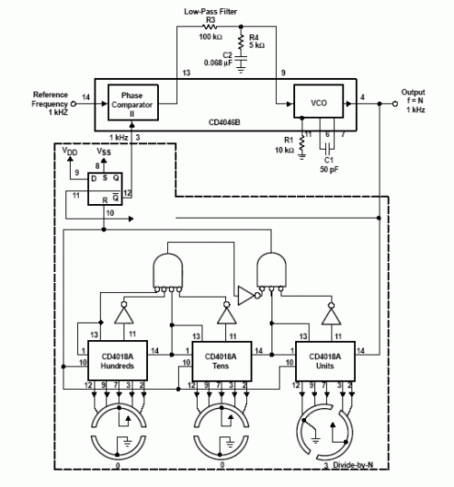
A frequency synthesizer circuit diagram has been found, but clarification is needed regarding a component connected to VDD from pin 9, VSS from pin 8, and pin 12, which is linked to the phase comparator 2. The component in...