
FUNCTION GENERATOR

The described circuit is a waveform generator capable of producing both square and triangle wave outputs. The primary function of the left section of the circuit operates similarly to a comparator, utilizing positive feedback to introduce hysteresis. This configuration ensures that the circuit can switch states cleanly and provides stability against noise.
In this circuit, the inverting input of the comparator is set to a reference voltage, precisely half of the supply voltage (Vcc), achieved through the voltage divider formed by resistors R4 and R5. This configuration allows the circuit to toggle between high and low states based on the input signal's amplitude, effectively controlling the output frequency.
The output of the comparator feeds back to the non-inverting input, creating a feedback loop that influences the frequency of oscillation. The square wave output exhibits an amplitude of 8V peak-to-peak, indicating that the circuit is designed to operate within a specified voltage range, which is critical for applications requiring precise signal levels.
The second stage of the circuit functions as an integrator, utilizing an operational amplifier (op-amp) to convert the square wave output from the first stage into a triangle wave. The integration process is facilitated by resistor R3, which serves as the input element, while capacitor C1 acts as the feedback component. The values of R3 and C1 determine the integration time constant, which directly influences the slope of the triangle wave output.
Furthermore, the ratio of resistors R1 and R2 plays a vital role in setting the frequency of oscillation and, consequently, the characteristics of both the square and triangle wave outputs. Adjusting these resistor values allows for tuning the circuit to achieve desired frequency ranges and waveform properties, making it suitable for various applications in signal processing, waveform generation, and modulation systems. The circuit has both square-wave and triangle-wave output. The left section is similar in function to a comparator circuit that uses positive feedback for hysteresis. The inverting input is biased at one-half the Vcc voltage by resistor R4 and R5. The output is fed back to the non-inverting input of the first stage to control the frequency. The amplitude of the square wave is the output swing of the first stage, which is 8V peak-to-peak. The second stage is basically an op amp integrator. The resistor R3 is the input element and capacitor C1 is the feedback element. The ratio R1/R2 sets th 🔗 External reference
Related Circuits
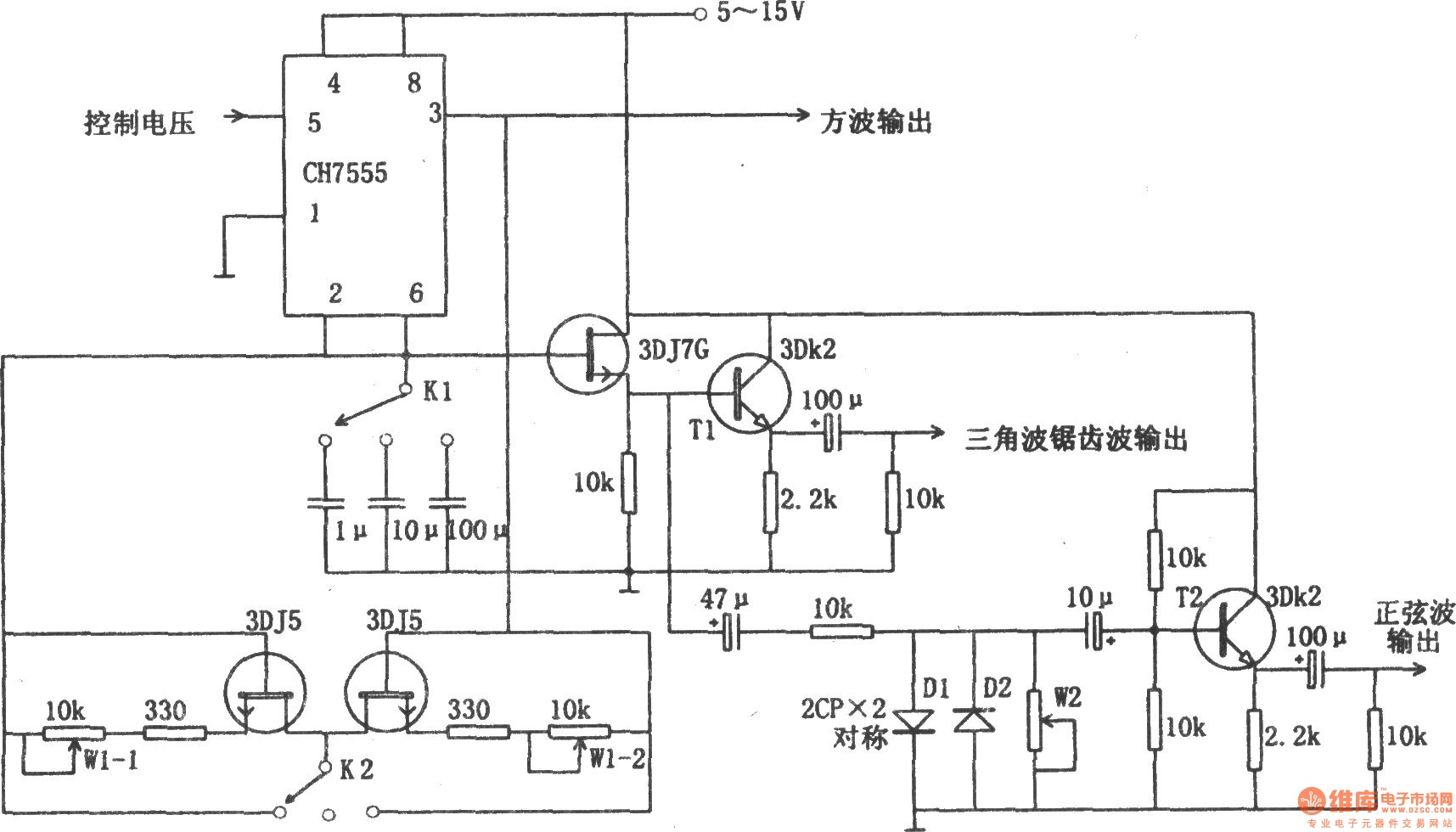
The chart illustrates a function generator circuit utilizing a 555 timer. This circuit includes a CH7555 timer along with several transistors and RC components. It is capable of generating triangle waves, square waves, sine waves, sawtooth waves, and square...
A simple buzzer is being converted into an oscillating buzzer to produce a sound similar to that of an automobile's reverse indicator. The schematic provided is borrowed from electroschematics.com. The intention is to replace the LED in the circuit...

The circuit depicted in Figure 3-168 utilizes a controller for speed grading and reversing control. A reverse brake is connected to the rotor circuit through an overcurrent relay, labeled KI, for control. The current relay KIi to KI3 serves...
Set R5 to read 1V RMS on an audio millivoltmeter connected to the output with R7 rotated fully clockwise, or to view a sine wave of 2.828V peak-to-peak amplitude on the oscilloscope. An audio amplifier is an electronic device...
The first positive pulse from a classic 555-based oscillator is always 1.6 times longer than the subsequent pulses. This discrepancy occurs because, during the initial cycle, capacitor C2 begins charging from 0 V. While this is typically not an...
Multi Tone Alarm Description This is a simple and easy-to-build multi-tone alarm circuit that can be used in burglar alarms or sirens. The circuit is based on the dual op-amp MC1458 and LM380. The two op-amps inside the MC1458...