
555 Pulse generator
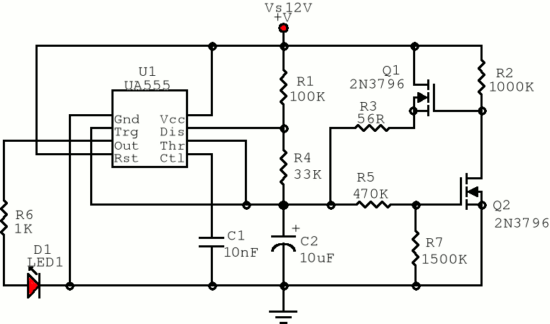
The described circuit utilizes a classic 555 timer configured in astable mode, generating a square wave output. The first pulse's extended duration is a common characteristic of such configurations due to the initial charging behavior of capacitor C2. The addition of Q1 and Q2, along with resistors R3, R5, and R7, provides a mechanism to normalize the pulse lengths.
Upon powering the circuit, C2 starts from a discharged state, causing Q2 to remain off initially. The rapid charging of C2 through Q1 and R3 allows the circuit to quickly transition into its regular oscillation pattern. The selection of R5 and R7 is crucial; these resistors form a voltage divider that determines the gate voltage of Q2 based on the voltage across C2. The optimal ratio ensures that Q2 turns on just as C2 approaches the threshold of Vs/3, allowing for a smooth transition to the normal operating mode of the oscillator.
The behavior of the circuit is sensitive to component values, particularly the resistance values of R5 and R7. If R5 is too high, it may prevent Q2 from turning on, while a low R7 may cause premature activation. The design should therefore aim for a balance that allows for effective charging and discharging of C2 while maintaining stable oscillator operation. The cumulative resistance of R5 and R7 should be kept high to minimize interference with the main oscillator circuit, ensuring that the performance is not compromised after the first pulse. This careful consideration of component values and their interactions is essential for achieving the desired functionality of the modified 555 oscillator circuit.The first positive pulse from a classic 555-based oscillator is always 1. 6 times longer than the following pulses. The difference is caused by the fact that only during the first cycle C2 starts charging up from 0 V. This is generally not a problem, but sometimes this first pulse just should be the same length as the rest - at least approximately.
The picture shows the oscillator and an addition to it (everything to the right from the Vs-Gnd axis) that can solve the problem. Immediately after switch-on, C2 is empty and the voltage on the gate of Q2 is low. Q2 is off and it makes C2 charge up very quickly through Q1 and R3 until it reaches just below Vs/3. Then Q2 turns on, Q1 turns off, and the classic circuit continues to charge and discharge C2 relatively slowly between 2Vs/3 and Vs/3.
As the voltage on C2 never again drops below Vs/3, Q2 now conducts all the time and Q1 is permanently off. The component values may be critical. For best results, the R5/R7 voltage divider should turn Q2 on when C2 is charged up to just a little below Vs/3.
This point is set by the R5/R7 ratio. But if the value of R5 is too high or if R7 is too small (depending on the supply voltage and the G-S threshold voltage of Q2), the oscillator may not work at all. The sum of R5 and R7 should be as high as possible in order to minimize the influence on the main part of the circuit after the first pulse.
🔗 External reference
Related Circuits
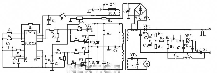
The circuit utilizes the SC3525A, a PWM silicon chip from US General Semiconductor. It features an error amplifier with an inverting input at pin 1. Pin 2 serves as the non-inverting input for the error amplifier. Pins 5 and...
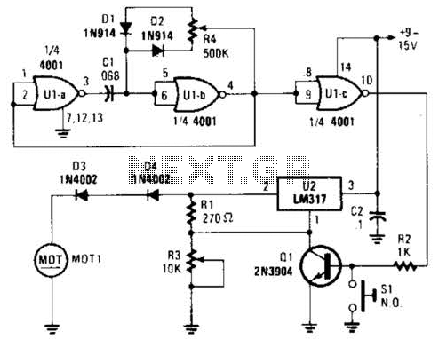
Connected in this manner, an LM317 1-A adjustable-voltage regulator can be utilized to control the speed of a miniature DC motor or to adjust the brightness of a small lamp. The circuit achieves this by modulating the pulse width,...

A tapped-coil Colpitts oscillator is utilized at Q1 to deliver four tuning ranges: 1.7 to 3.131 MHz, 3.0 to 5.6 MHz, 5.0 to 12 MHz, and 11.5 to 31 MHz. A Zener diode (D2) is incorporated at Q1 to...
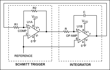
This application note describes the implementation of a single-supply triangular wave oscillator using the MAX9000 integrated circuit and several passive components. The circuit employs an operational amplifier, a comparator, and a voltage reference as the main active components. The...
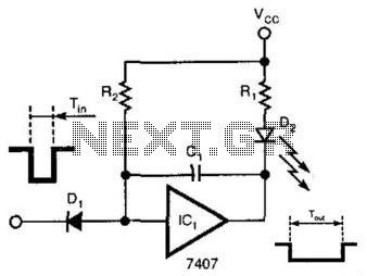
A single gate (open collector, non-inverting) generates a simple one-shot pulse that lasts for a duration equal to t, plus the RiCi time constant. R2 serves as a pull-up resistor to maintain the input of the gate high while...
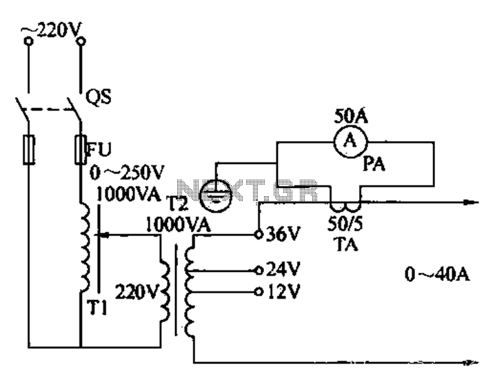
Electricians sometimes use overcurrent relays, thermal relays, and other devices to perform periodic overcurrent checks with a current generator. A secure running lights transformer, voltage regulator, and meter can be constructed using a small electric current generator. The homemade...