
Fundamentals of Electrical Engineering and Class B audio amplifier
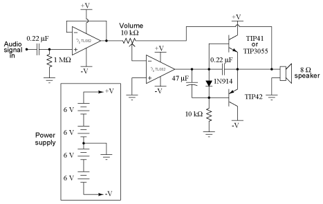
The described audio amplifier circuit employs TIP41 and TIP42 transistors, which are well-suited for this application due to their matched characteristics and power handling capabilities. The circuit design focuses on achieving high fidelity in audio reproduction while maintaining efficiency. The push-pull configuration facilitates the amplification of both halves of the audio waveform, enhancing sound quality by minimizing distortion.
The circuit can be constructed on a printed circuit board (PCB) or a breadboard, with careful attention to component placement to reduce noise and interference. The input stage typically includes a coupling capacitor to block DC offsets from the audio source, ensuring that only the AC audio signal is amplified. Feedback mechanisms may also be integrated to stabilize gain and reduce distortion further.
Power supply design is critical; a dual power supply configuration (+V and -V) is often used to accommodate the push-pull nature of the circuit. Decoupling capacitors should be placed close to the power supply pins of the transistors to filter out high-frequency noise, ensuring stable operation.
Thermal management is essential, especially in a class B amplifier where transistors operate near their limits. Heat sinks may be utilized, and proper ventilation must be considered in the overall design to prevent thermal runaway conditions. Testing and tuning the biasing of the transistors will be necessary to optimize performance and minimize crossover distortion while ensuring that the amplifier operates efficiently and reliably.
In summary, this audio amplifier circuit represents a practical implementation of class B amplification principles, aimed at delivering quality audio output with efficient power usage. Proper attention to component selection, circuit layout, and thermal management will contribute to achieving the desired performance characteristics.If possible, try to obtain TIP41 and TIP42 transistors, which are closely matched NPN and PNP power transistors with dissipation ratings of 65 watts each. If you cannot get a TIP41 NPN transistor, the TIP3055 (available from Radio Shack) is a good substitute.
Do not use very large (i. e. TO-3 case) power transistors, as the op-amp may have trouble driving enough current to their bases for good operation. This project is an audio amplifier suitable for amplifying the output signal from a small radio, tape player, CD player, or any other source of audio signals.
For stereo operation, two identical amplifiers must be built, one for the left channel and other for the right channel. To obtain an input signal for this amplifier to amplify, just connect it to the output of a radio or other audio device like this: This amplifier circuit also works well in amplifying "line-level" audio signals from high-quality, modular stereo components.
It provides a surprising amount of sound power when played through a large speaker, and may be run without heat sinks on the transistors (though you should experiment with it a bit before deciding to forego heat sinks, as the power dissipation varies according to the type of speaker used). The goal of any amplifier circuit is to reproduce the input waveshape as accurately as possible. Perfect reproduction is impossible, of course, and any differences between the output and input waveshapes is known as distortion.
In an audio amplifier, distortion may cause unpleasant tones to be superimposed on the true sound. There are many different configurations of audio amplifier circuitry, each with its own advantages and disadvantages. This particular circuit is called a "class B, " push-pull circuit. Most audio "power" amplifiers use a class B configuration, where one transistor provides power to the load during one-half of the waveform cycle (it pushes) and a second transistor provides power to the load for the other half of the cycle (it pulls).
In this scheme, neither transistor remains "on" for the entire cycle, giving each one a time to "rest" and cool during the waveform cycle. This makes for a power-efficient amplifier circuit, but leads to a distinct type of nonlinearity known as "crossover distortion.
" If the "hand-off" between the two transistors is not precisely synchronized, though, the amplifier`s output waveform may look something like this instead of a pure sine wave: Here, distortion results from the fact that there is a delay between the time one transistor turns off and the other transistor turns on. This type of distortion, where the waveform "flattens" at the crossover point between positive and negative half-cycles, is called crossover distortion.
One common method of mitigating crossover distortion is to bias the transistors so that their turn-on/turn-off points actually overlap, so that both transistors are in a state of conduction for a brief moment during the crossover period: This form of amplification is technically known as class AB rather than class B, because each transistor is "on" for more than 50% of the time during a complete waveform cycle. The disadvantage to doing this, though, is increased power consumption of the amplifier circuit, because during the moments of time where both transistors are conducting, there is current conducted through the transistors that is not going through the load, but is merely being "shorted" from one power supply rail to the other (from -V to +V).
Not only is this a waste of energy, but it dissipates more heat energy in the transistors. When transistors increase in temperature, their characteristics change (Vbe forward voltage drop, ², junction resistances, etc. ), making proper biasing difficult. In this experiment, the transistors operate in pure class B mode. That is, they are never conducting at the same time. This saves 🔗 External reference
Related Circuits
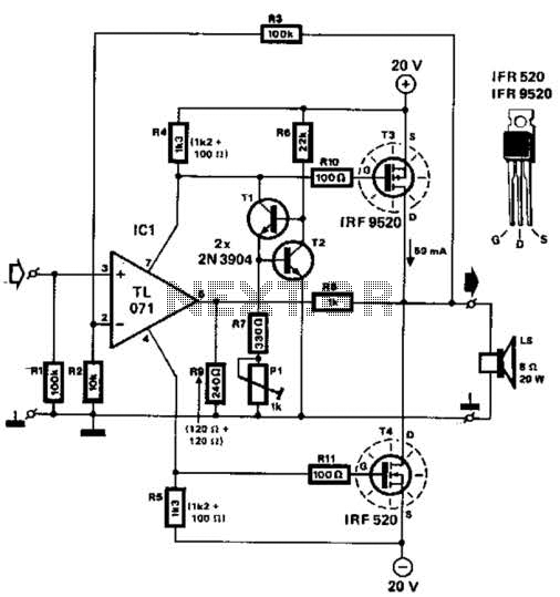
Two complementary MOSFETs are utilized to deliver 20 W into an 8-ohm load. A TL071 operational amplifier serves as the input amplifier. The MOSFETs must be equipped with a heatsink that has a thermal resistance of better than 5...
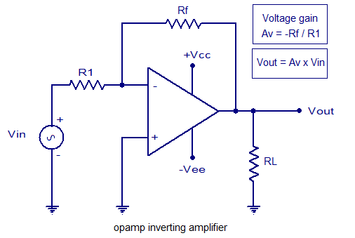
An inverting amplifier utilizing an operational amplifier (op-amp). This includes equations for voltage gain and output voltage, as well as input and output waveforms, and a practical inverting amplifier circuit using the 741 IC. An inverting amplifier is a fundamental...
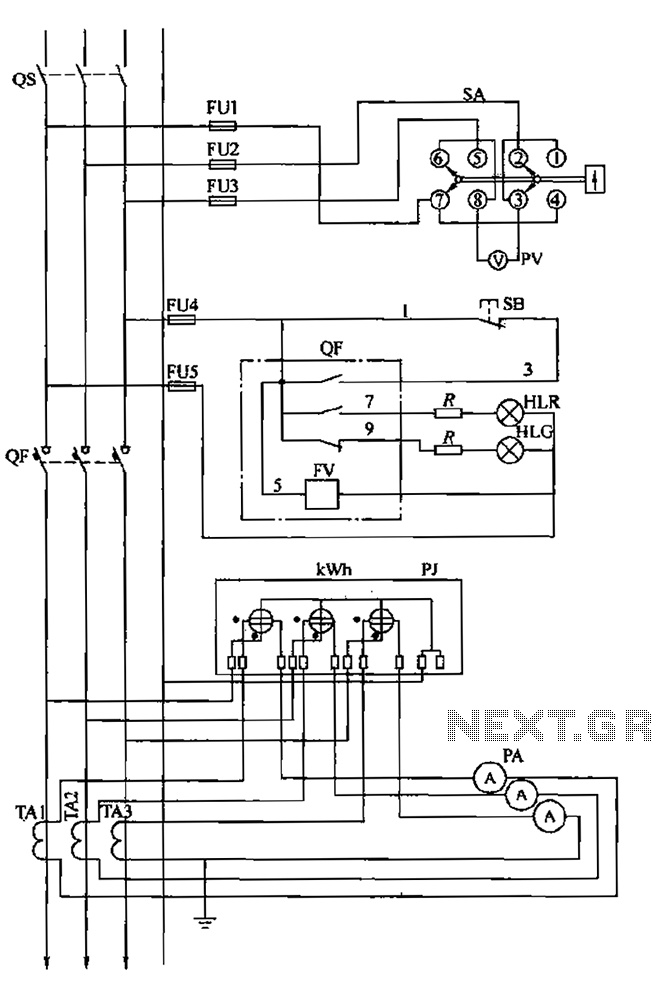
The BSL is illustrated in a low-voltage distribution panel wiring diagram. It consists of three main components: the voltage measuring circuit, secondary circuit protection, and the energy metering circuit. (1) The voltage measuring circuit includes a voltage switch (SA)...

The main component of the circuit has been achieved using an integrated circuit (IC) with a significant number of bulk components, primarily capacitors. The internal circuit is designed to output from the differential amplifier using a PNP unipolar configuration,...
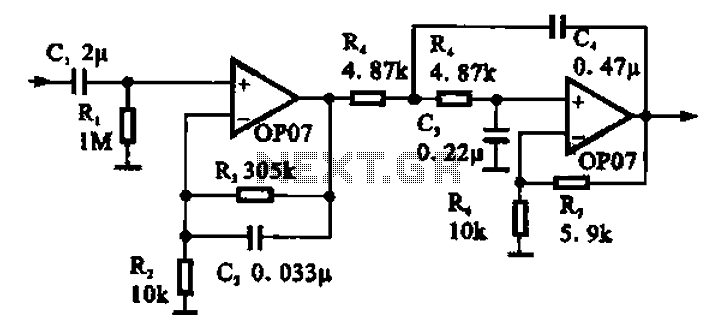
Broadband 0.1 to 10 Hz filter amplifier. The broadband circuit consists of two operational amplifiers configured as filter amplifiers operating in the frequency range of 0.1 to 10 Hz. The broadband filter amplifier circuit utilizes two operational amplifiers (op-amps) to...
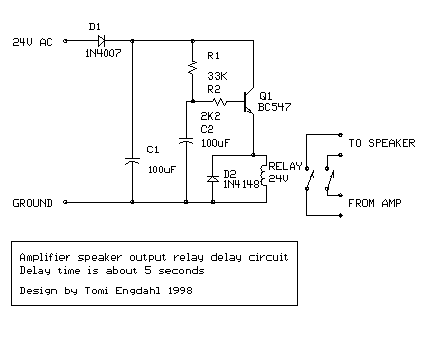
This is a simple circuit designed for an audio amplifier project to control the speaker output relay. The purpose of this circuit is to manage the delay that activates the relay, which connects the speakers to the audio amplifier....