
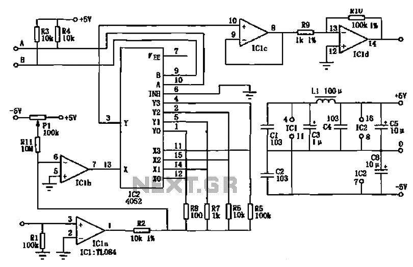
Gain amplifying circuit diagram or programming
The PGA103 operational amplifier is specifically engineered to accommodate a broad spectrum of input voltages, making it suitable for various applications where high voltage signals need to be processed. The implementation of a voltage divider using an 11.3kΩ resistor in conjunction with a 102kΩ resistor allows for precise scaling down of high input voltages. This configuration ensures that when subjected to a high input voltage, such as 120V, the resultant voltage presented to the PGA103 is safely reduced to 12V, thereby preventing damage to the amplifier and ensuring proper operation.
The choice of diodes D1 and D2, specifically the 1N4148 model, is critical for protecting the PGA103 from voltage spikes and reverse polarity conditions. These diodes are configured in a bidirectional arrangement to clamp the input voltage effectively, ensuring that the operational amplifier receives a maximum input voltage of 15V and a minimum of -0.7V. This clamping mechanism is essential for safeguarding the integrity of the PGA103's internal circuitry and maintaining its performance characteristics over varying input conditions.
Overall, the combination of the voltage divider and the clamping diodes plays a pivotal role in the reliable operation of the PGA103 in high-voltage environments, making this circuit design a robust solution for interfacing with high-voltage signals. As shown in FIG PGA103 constituted by a wide input voltage range of the amplifier. 11.3k with 102k resistor voltage divider circuit dividing ratio of about 1/10, such as when t he input voltage is 120V, after dividing the input voltage applied PGA103 only 12V, wide input voltage can be. At the same time, the diode D1, D2 (take 1N4148) play a two-way clamping action, PGA103 input voltage of 15 ~ disabilities 0.7V.
Related Circuits
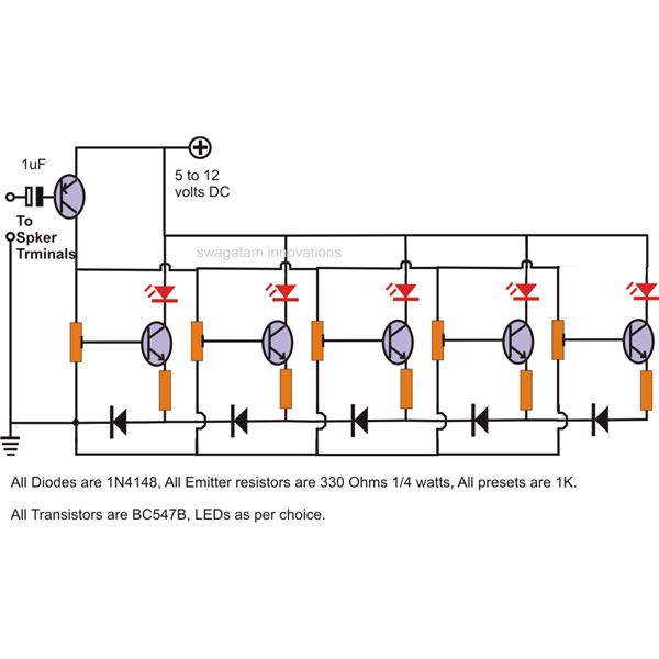
The LEDs in the circuit light up sequentially and "dance" in response to the music level applied at the input, preferably from the speaker terminals of the audio device being monitored. This configuration is consistent across all LEDs in...
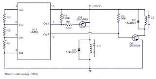
The values of the LM56 thermostat project circuit diagram for resistors R1, R2, and R3 at the travel points VT1 and VT2 can be determined using the following equations. This electronic circuit thermostat with the IC LM56 serves as...
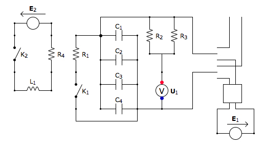
This is the discharging circuit. The red lines indicate the flow of energy from the capacitors to the terminals when the switch is in the upward position. The circuit is complete due to the connection of the terminals by...

This circuit must be used between the drive voltage of such a transformer and track. On JP1, the transformer is connected to JP2, the rails are connected to JP3, is a TTL "High" position when there is a tax...
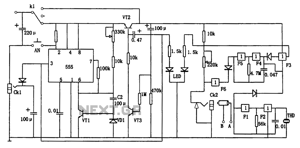
The circuit represents a general multi-function alarm and timing mechanism. Its timing capabilities range from 5 minutes to 3 hours. The timing components include C2, VD1, and VT1. The circuit utilizes a capacitance multiplier with a 555 timer. CK1,...
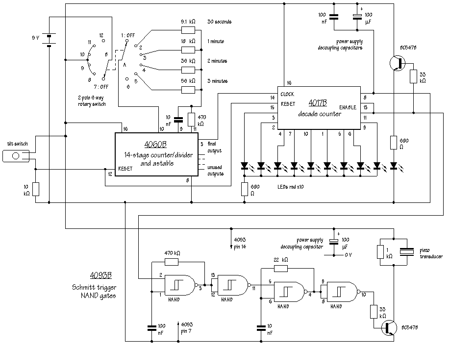
This is a game timer circuit diagram. When the game timer is reset, two actions must occur: the 4017 counter must return to zero, and the 4060... The game timer circuit utilizes the 4017 decade counter and the 4060 binary...