
Positive Voltage Doubler
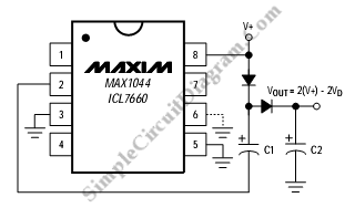
The Positive Voltage Doubler circuit is designed to convert a lower input voltage into a higher output voltage, effectively doubling the input voltage. The MAX1044 and ICL7660 are integrated circuits that facilitate this process through charge-pump technology. The operation of the circuit involves the use of capacitors and diodes to store and transfer charge, resulting in an increased output voltage.
In this configuration, the circuit typically consists of two capacitors, C1 and C2, and a Schottky diode, D1. The input voltage is applied to the circuit, and during the first phase of operation, capacitor C1 charges to the input voltage level. In the next phase, the switch within the IC alternates, allowing C1 to discharge into C2 while simultaneously charging from the input voltage again. The Schottky diode is crucial in this process as it allows current to flow in one direction with minimal voltage drop, thus improving efficiency.
The output voltage across C2 will be approximately double the input voltage, minus the forward voltage drop of the diode. This circuit is particularly useful in applications requiring higher voltages from a standard lower voltage source, such as powering operational amplifiers or other analog components that require a higher supply voltage. The choice of components, particularly the Schottky diode, is essential for optimizing performance and minimizing losses in the circuit.
Overall, the Positive Voltage Doubler circuit using the MAX1044 or ICL7660 is an effective solution for applications needing increased voltage levels while maintaining compactness and efficiency.This is a simple circuit of Positive Voltage Doubler. This circuit uses the MAX1044/ICL7660. The schottky diode was chosen to reduces the voltage drop. This.. 🔗 External reference
Related Circuits
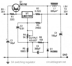
The circuit diagram presented is a simple and cost-effective switching voltage regulator capable of delivering an adjustable output voltage range from 1.8V to 32V with a maximum static current of 3A. This regulator utilizes the adjustable LM317HV IC along...

NiCd charger with current and voltage limiting power supply. This is a car NiCd battery charger circuit that can charge any Ni-Cd battery between 4.8 and 4.4 volts from a classic 12 volts car battery. The charging current can...
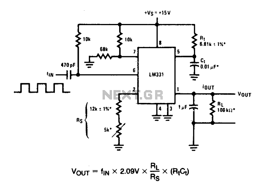
In these applications, a pulse input at a specified percentage is differentiated by a capacitor-resistor (C-R) network. The negative-going edge at pin 6 triggers the input comparator, activating the timer circuit. Similar to a voltage-to-frequency (V-to-F) converter, the average...
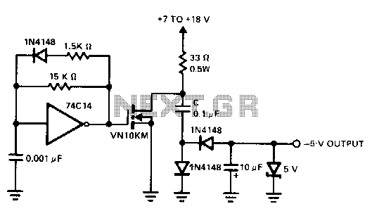
A charge pump is a straightforward method for generating a low-power voltage supply of opposite polarity from the main supply. The 74CL4 IC serves as a self-oscillating driver for the MOSFET power switch, producing a pulse width of 6.5...

AVR has two different programming modes called Parallel Programming Mode (Parallel Mode) and Serial Downloading Mode (ISP mode). In Parallel Mode, the programming is done using multiple data lines simultaneously, allowing for faster programming speeds. This mode is typically...
This circuit regulates a DC power output and has a wide range of applications. It can be utilized to control the speed of a motor, a pump, a toy train, or the brightness of an LED or lamp. Essentially,...