
Generate Dual Voltages That Track By Percentage Of Range
The described circuit effectively addresses the challenge of generating multiple tracking voltages with high accuracy. The use of a square-wave oscillator to create triangular waveforms allows for precise control over the output voltages. The choice of a single potentiometer to adjust the duty cycle is a significant improvement over traditional ganged potentiometers, reducing the likelihood of tracking errors. The integration of the output pulses ensures that the resulting voltages are smooth and stable, critical for applications requiring precise voltage control.
Transistor Q1 plays a pivotal role in shaping the output pulses, ensuring that the transitions are sharp and well-defined, which is essential for maintaining the integrity of the signals processed by the analog multiplexer. The multiplexer itself allows for the selection of different voltage levels, enabling the circuit to adapt to various requirements without the need for multiple independent potentiometers.
The design emphasizes the importance of component selection, particularly the use of low-leakage capacitors, which are vital for maintaining the accuracy of the integrator outputs. The specified frequency of 5 kHz strikes a balance between minimizing ripple and ensuring fast response times, making the circuit suitable for dynamic applications where voltage adjustments are frequently required.
Overall, this circuit exemplifies a robust solution for generating multiple tracking voltages with high precision, making it applicable in various electronic systems where voltage regulation is critical. The potential for expansion with additional components further enhances its versatility and utility in complex electronic designs.Consider the need to vary two voltages, V1 and V2, by an equal percentage of their ranges (V1MAX - V1MIN) and (V2MAX - V2MIN), with V1MAX, V1MIN, V2MAX, and V2MIN independent of each other. The first idea that comes to mind is to use ganged potentiometers (Fig. 1). However, ganged potentiometers are notorious for producing tracking errors as high as 5%. Here`s a simple method that uses a single potentiometer to generate two or more tracking voltages with an accuracy of better than 0. 5% of range (Fig. 2). The circuit around IC1a is a square-wave oscillator. Triangular waves across C1 are applied to comparator IC1b. Potentiometer P1 varies the duty cycle of the pulses at the comparator output from 0% to 100%. Transistor Q1 and the multiplexer switch IC2 convert the comparator output into pulses with well defined edges.
These pulses are applied to the digital control inputs of the analog multiplexer that receives V1MAX, V1MIN, V2MAX, and V2MIN as the analog inputs. The multiplexer outputs, which are integrated by components R7-C2 and R8-C3, are buffered by IC1c and IC1d.
The oscillator`s frequency is optimized to be about 5 kHz. This frequency is high enough to produce negligible ripple in the integrator output. At the same time, the frequency is low enough to ensure that rise and fall times of the pulses are negligible compared to the pulse repetition period. Note that capacitors C2 and C3 must be low-leakage types. This idea can be extended to generate more tracking voltages by using additional multiplexer switches, integrators, and buffers.
🔗 External reference
Related Circuits
In daily life and production, many situations such as vehicle rollback, robot obstacle avoidance, industrial well logging, and liquid level measurement in reservoirs require non-contact automatic distance measurement. Ultrasonic waves refer to sound waves produced by machinery in an...
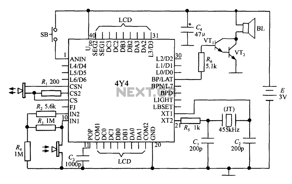
The 4Y4 is a monolithic liquid crystal display rangefinder circuit. The instrument comprises an ultrasonic transmitter, a receiver, an LCD display, buttons, switches, and a buzzer (or speaker). To simplify wiring, the 4Y4 is directly welded to the back...
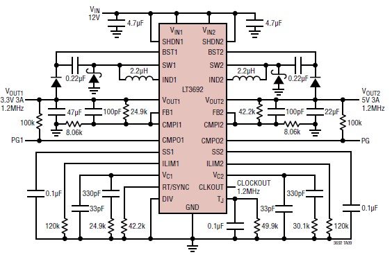
The LT3692 dual current mode PWM step-down DC-DC converter circuit, featuring two internal 3.5A switches, can be utilized to design a straightforward power supply circuit suitable for various electronic applications, including distributed supply regulations and automotive circuits. The LT3692...
Most amplifiers operate at acoustic frequencies, sometimes requiring two or even three transformers instead of a single power transformer. This approach is more prevalent in high-end amplifiers, where enthusiasts often prioritize high fidelity over cost. In these setups, the...

A device such as burglar alarms and sirens, whose basic purpose is to monitor a tested circuit diagram with a description of a burglar alarm using a dual operational amplifier. The burglar alarm system utilizes a dual operational amplifier (op-amp)...

This FM transmitter project is a simple yet effective circuit capable of transmitting signals over a distance of up to 1 kilometer in open air conditions. The circuit employs an RF transistor in the output stage, along with two...