
Glitch-Free Clipper
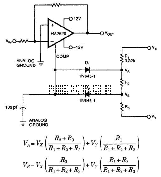
The described clamping circuit enhances the functionality of the Harris 2620 op-amp by preventing distortion and ensuring signal integrity during high-voltage excursions. The high-impedance input pin is critical for maintaining the op-amp's performance characteristics, allowing it to accurately track the output voltage while minimizing loading effects. The diodes D1 and D2 serve as the primary clamping elements, allowing the output voltage to remain within the specified limits, thereby protecting the downstream circuitry from overvoltage conditions.
The selection of resistors R1, R2, and R3 is essential for setting the appropriate clamping levels and ensuring the desired response time of the circuit. By adjusting R1, the values of R2 and R3 can be fine-tuned, impacting the dynamic range and response of the clamping action. The recommended value of R1 at around 3 kΩ is a starting point that can be optimized based on the specific application requirements.
The performance of the clamping circuit can be assessed by examining the total harmonic distortion (THD) across a range of frequencies. The reported THD of less than -75 dB demonstrates the circuit's effectiveness in preserving signal quality, even with a sinusoidal input at 30 kHz. This level of performance indicates that the circuit is well-suited for audio applications and other scenarios where signal fidelity is paramount.
In practical implementation, the clamping circuit should be carefully laid out to minimize parasitic capacitance and inductance, which could affect the response time and overall performance. Additionally, the choice of diodes D1 and D2 should consider their switching speed and forward voltage drop to ensure optimal clamping action.
Overall, the integration of this clamping circuit with the Harris 2620 op-amp provides a robust solution for applications requiring precise voltage control and protection against signal distortion, enabling reliable operation in demanding electronic environments. Adding a simple clamping circuit to a Harris 2620 high-speed op amp produces a glitch-free amplifier/ clipper. The op a mp pin that controls the device"s bandwidth is a high-impedance, isolated input. This pin also tracks the device"s output voltage. Therefore, Dl, D2, RI, R2, and R3 will clamp the amplifier"s output voltage only when the amplifier"s input voltage exceeds your clamping-voltage limits. VD is the diode drop of Dl or D2. where Vx and Vy are the clamping circuit"s bias voltages. Choosing R lets you determine the values of R2 and R3. Try a value for Ri around 3 kfi. One example of this circuit had clamping voltages of ± 3.7 V and exhibited THD below - 75 dB for a sinusoidal, 30-kHz input signal.
When the input signal increased beyond the ± 3.7-V clamping voltage, the clipper symmetrically clamped the output voltage with no glitches in the waveform. 🔗 External reference
Related Circuits
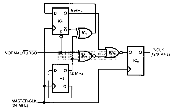
This circuit generates a dual-speed clock for personal computers. It synchronizes asynchronous switch inputs with the master clock to provide glitch-free transitions between clock speeds. The dual-speed clock allows certain programs to operate at a higher clock speed for...
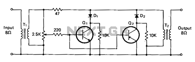
T1 and T2 are 600 to 8-ohm transformers (any transistor radio output transformers with 500 to 4-ohm impedance may be used). Q1 is a 2N2222 NPN transistor, and Q2 is a 2N2907 PNP transistor. D1 and D2 are 1N270...

For use with headphones, this circuit sets the audio clipping level via a 5-kOhm potentiometer. This type of noise clipper is most effective for pulse-type noise with a low duty cycle, such as ignition noise. The resistor Rl establishes...
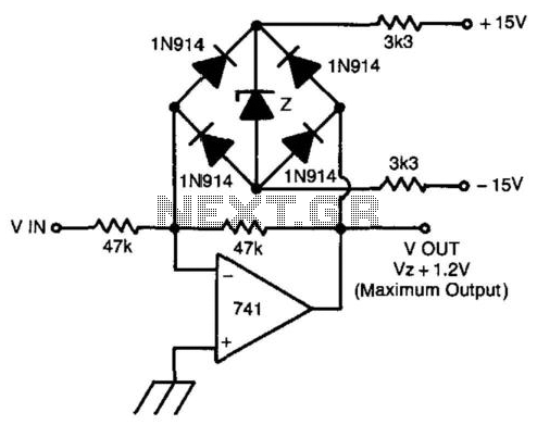
The issue with utilizing two Zener diodes in series for symmetrical clamping is that the knee of the Zener characteristics is imprecise. Additionally, charge storage within the Zeners can lead to speed issues, and the Zeners may exhibit slightly...
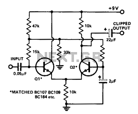
A differential amplifier serves as an effective audio clipper, capable of delivering precise and symmetrical clipping. The circuit presented begins clipping at an input voltage of 100 mV, with the output starting to clip at ±3 V. For optimal...
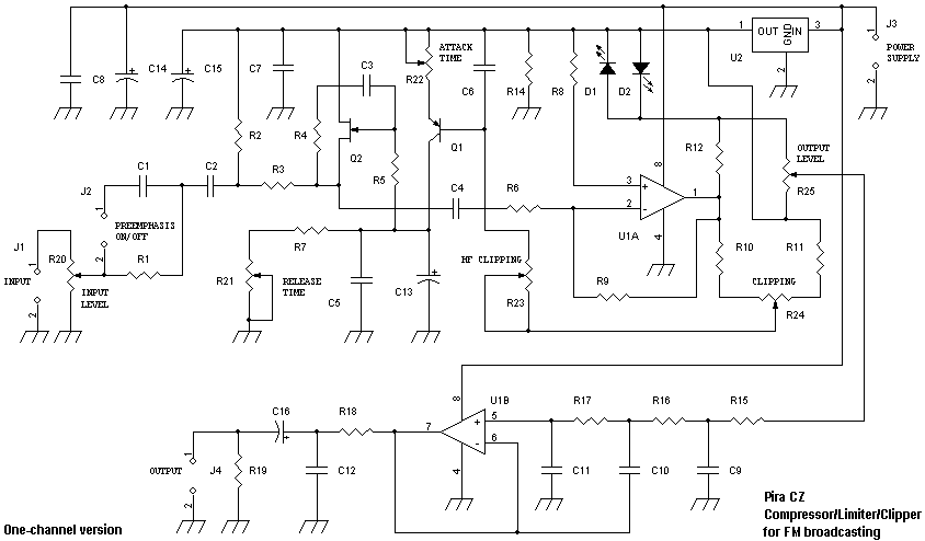
Audio signals as music or speech have big dynamic ranges. There are silent and loud sections. These audio signals aren't too good for a transmitter, which requires audio signal with constant level on the input. Limiter is a device,...