
Graphic Equalizer Circuit for 10 Frequency Bands
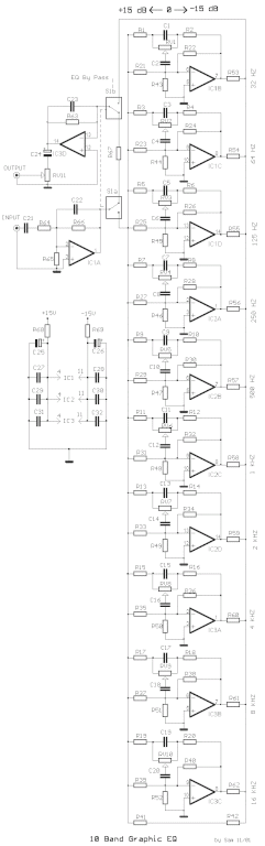
The described circuit is a graphic equalizer that utilizes a multi-band approach to audio signal processing. It is structured to divide the audio spectrum into ten distinct frequency bands, allowing for individual adjustment of each band. This is typically achieved using a series of bandpass filters, each tuned to a specific frequency range.
The design incorporates operational amplifiers (op-amps) for signal amplification and filtering, ensuring that the audio signal maintains its integrity while being processed. The output of each bandpass filter is routed to a control interface, often consisting of sliders or knobs, which allow the user to boost or cut the gain of each frequency band.
This configuration enables precise control over the audio output, allowing users to tailor the sound to their preferences or to compensate for deficiencies in the audio playback environment. The circuit also includes a master output stage that combines the adjusted signals from all ten bands, ensuring that the final output maintains a balanced and coherent sound.
Power supply considerations are crucial in this design, as the circuit must provide stable voltage levels to the op-amps and other active components to prevent distortion. Additionally, careful layout and grounding techniques are necessary to minimize noise and interference, which can adversely affect the audio quality.
In summary, the circuit's design focuses on flexibility and precision in managing audio frequencies, making it suitable for various applications in music production, live sound reinforcement, and home audio systems.The circuit was designed to create ten different frequency bands to be handled by a single graphic equalizer to produce and maintain a predetermined area.. 🔗 External reference
Related Circuits
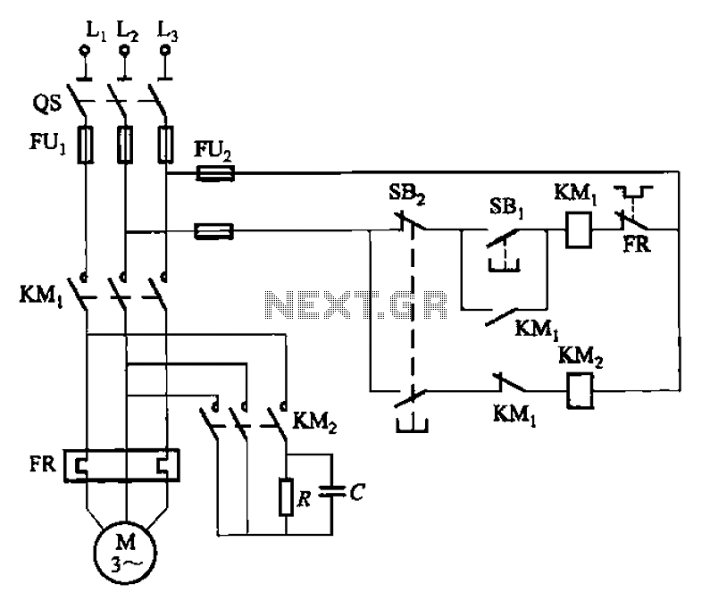
The 3F155 circuit, as depicted in the provided figure, operates in manual control mode. It features a self-excitation braking phase, while the other two phases utilize a short brake. A resistor (R) is involved, along with the voltage across...
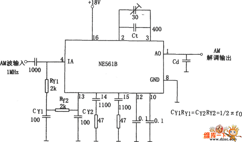
The figure illustrates a bilateral band modem circuit utilizing the NE561B component. The input modulating signal operates at a loading frequency of f0 = 1 MHz. When the AM modulation signal is applied to the input terminal of the...
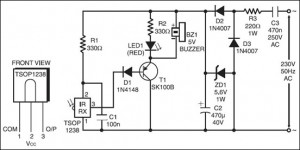
The following circuit illustrates an IR Remote Control Tester Circuit. Features include that transistor T1 conducts during the negative pulse period, and there is a data output pin. The IR Remote Control Tester Circuit is designed to verify the functionality...
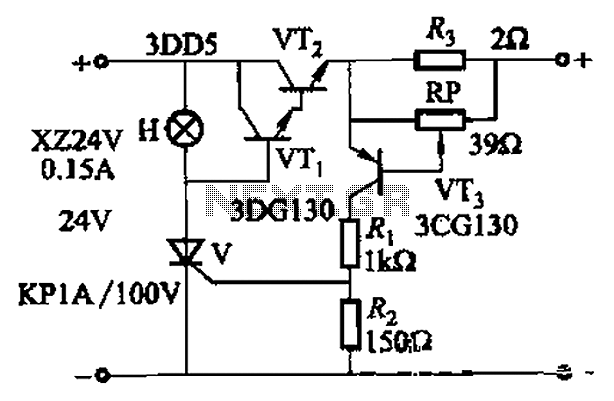
By adjusting Ro or RP, the current setpoint can be modified. The circuit illustrated in Figure 14-98 features overcurrent protection using a thyristor and transistors VTi and VT2, which immediately cut off the power when an overcurrent condition is...
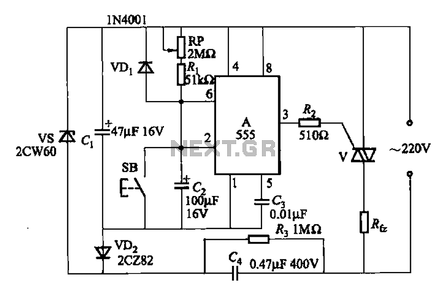
A 555 four-base integrated circuit delay circuit is designed to facilitate a transition from high to low output. When the button SB is pressed, the output is set to high, and after a specified delay, the output transitions to...
A DSB transmitter is significantly less expensive to construct compared to an SSB transmitter since it does not require filters or phasing networks. This circuit can generate an output of up to 1 watt on the 10-meter band. The...
Warning: include(partials/cookie-banner.php): Failed to open stream: Permission denied in /var/www/html/nextgr/view-circuit.php on line 713
Warning: include(): Failed opening 'partials/cookie-banner.php' for inclusion (include_path='.:/usr/share/php') in /var/www/html/nextgr/view-circuit.php on line 713