
Guitar Effects & JFET Splitter
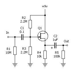
This JFET buffer circuit is designed for versatility and ease of use in audio applications, effectively serving as both a buffer and a splitter. Its high input impedance ensures minimal loading on the guitar's pickups, preserving tonal integrity while allowing for multiple outputs. The option to modify resistor values provides flexibility in tailoring the circuit's response to suit individual preferences. The incorporation of mute switches adds further control over the output signals, enhancing the circuit's functionality in live or studio settings. The straightforward construction and adaptability of this buffer/splitter make it an excellent choice for musicians and audio engineers alike, facilitating seamless integration into various setups.This is the schematic of a simple jfet buffer from the Basic Buffers article in the AMZ Lab Notebook, with the addition of pulldown resistors at the input and output. The circuit has a high input impedance and a low output impedance suitable for driving long cable runs or low impedance pedal inputs.
Current draw is low and it is quiet and simple t o construct. A stripboard (veroboard) layout and a pcb design are included in the original article about this circuit. I was looking at the article for the buffer and realized how easy it would be to extend the circuit so that it is a signal splitter.
a high impedance input buffer but with multiple independent outputs. All that is required is to parallel extra source follower units with the original. As you can see here, two more fets have been added to the original circuit. Each has separate low impedance drives from their source connections. Since the gate junction of a jfet is extremely high impedance, it does not change the input characteristics of the buffer circuit when additional transistors are put in parallel. With three totally independent buffered outputs, one can be dedicated to a tuner while the remaining two may be used to drive stereo pedal inputs or even two separate amplifiers.
This splitter would work great at the input of your pedal chain, immediately after the guitar so that the pickups are loaded by the high impedance of the buffer/splitter. If you want to change the input impedance, the values of R2 and R3 can be altered to suit your taste.
If the signal seems too crisp and bright, lower the values of those two resistors to 470k each. Always keep R2 equal to R3. It is not necessary to use all three outputs. If you have a need for only two, leaving the output jack of the third buffer without a plug in it will not cause a problem. One more option would be to add a mute switch to any output that you need to be able to silence. As an example, if you want to be able to turn off Out3, you could connect an SPST in parallel with the R9 resistor.
When open, the output performs as normal. When the switch is closed, output 3 is pulled to ground and no signal passes. Similar switches could be added across the Out1 and Out2 pull-down resistors if desired. It is easy to modify the stripboard layout of the original buffer to accomodate the additional jfet sections. The gate and drain leads of each of the jfets are in parallel so only the source has to be isolated. The four red boxes with red dots in the middle are places where the copper stripboard traces have to be cut to make the circuit function properly.
These cuts will isolate the source connections of the transistors. Just cut away the copper while leaving the epoxy substrate intact. If you want to make a pc board for the splitter, I have these images available for download: PC Board and PCB parts placement. The pcb board is the same basic layout as the stripboard. Source follower buffers are not too demanding about the choice of transistor so any jfet that you have in your parts bin would work in this circuit.
Typical devices that I would suggest here are the J201, 2N5457, 2N5486, 2N3819, MPF102, BF245, 2SK117, 2SK130 and similar parts. 🔗 External reference
Related Circuits

This preamplifier is designed as a portable unit, ideal for amplifying signals generated by guitar pickups, particularly the "bug" types used with acoustic instruments. It can be utilized with any type of device and pickup. The unit features a...
A 4x10" Ashdown ABM bass cabinet is powered by a Hughes & Kettner bass amplifier head. There is an intention to modify the amplifier head to enhance its functionality. The Ashdown ABM bass cabinet features four 10-inch speakers, which are...
This sound effects circuit is designed to function as a signal distorter. When utilized with an electric guitar, it enables the creation of unique sound effects. The sound effects circuit operates by manipulating the input audio signal from the electric...
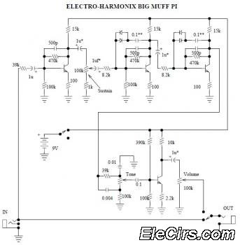
The Electro Harmonix Big Muff Pi circuit would likely benefit from the incorporation of a modern input-jack power connection and a DPDT bypass switch. The specific types of transistors and diodes used in the circuit are not specified. It...
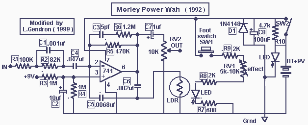
These two projects, Wah and Fuzz, are the results of a modification to a Morley dual channel volume control pedal that one of my sons suggested I undertake as he had no use for the volume unit but thought...

A simple linear voltage-controlled amplifier can be constructed with one operational amplifier (op amp) and two junction field-effect transistors (JFETs). This amplifier can achieve an 80-dB dynamic control range with less than ±0.2% linearity error for 0 V. The described...