
Guitar noise circuit diagram

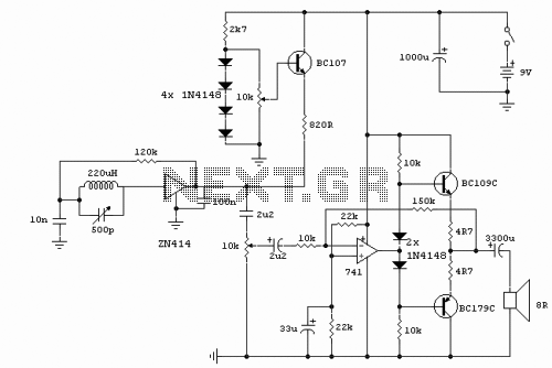
The described circuit leverages the operational amplifier (op-amp) model 741, known for its versatility in various applications. The maximum theoretical gain of the 741 is 20,000; however, in this design, the op-amp is configured to achieve an extraordinary gain of 2.7 million. This excessive gain can lead to significant output distortion, primarily due to noise interference, which is common in high-gain amplifier circuits.
To mitigate the distortion effects, the circuit incorporates two clamping diodes. These diodes function to prevent the output voltage from exceeding certain levels, thereby reducing the likelihood of clipping and maintaining signal integrity. The clamping action helps to stabilize the output, ensuring that the amplifier operates within a linear range.
Additionally, two other diodes are included in the design to influence the gain characteristics of the circuit. These diodes play a crucial role in shaping the frequency response and enhancing the overall performance of the amplifier. The combined effect of the clamping and gain-modifying diodes results in a circuit capable of generating a new sound profile while still preserving the nuances of the original audio signal.
The circuit's design is particularly useful in audio applications where maintaining sound quality is paramount. It can be employed in various audio processing tasks, such as effects units or sound synthesis, where both the manipulation of sound and fidelity to the original source are desired. Careful consideration of component selection and circuit layout will further enhance performance and minimize unwanted artifacts in the output. Circuit Description: The maximum gain circuit 741 to 20000, but the design of the circuit while filling a gain of 2.7 million, and then causes the output distortion. This disto rtion caused by noise effects. Two clamping diodes to reduce output low, while the two diodes that points multiplier impact becomes low. Since the sandwich will produce a new sound, the circuit can also be used to maintain the original sound.
Related Circuits
This receiver, designed around the popular ZN414 integrated circuit, operates within the AM band frequency range of 550 to 1600 KHz. For Longwave reception, it is necessary to replace the coil, which can be sourced from an old medium...
Due to the recent launch of Cranial Electrotherapy Stimulation (CES) portable devices in Europe, a similar circuit has been designed for hobbyists. CES is a widely used method for electrically enhancing brain function and has been prescribed by medical...
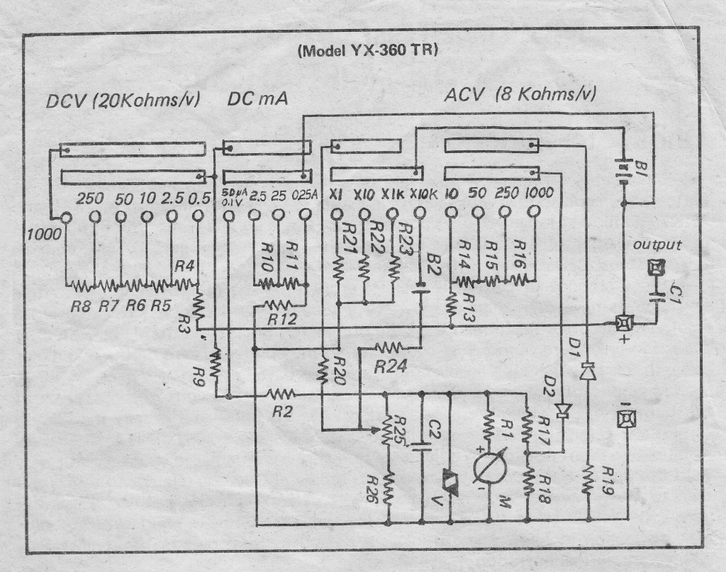
For individuals seeking a copy of the schematic diagram for this type of Analog Multitester, as well as other brands utilizing the same circuit diagram. The schematic diagram of an Analog Multitester typically features a variety of components arranged to...
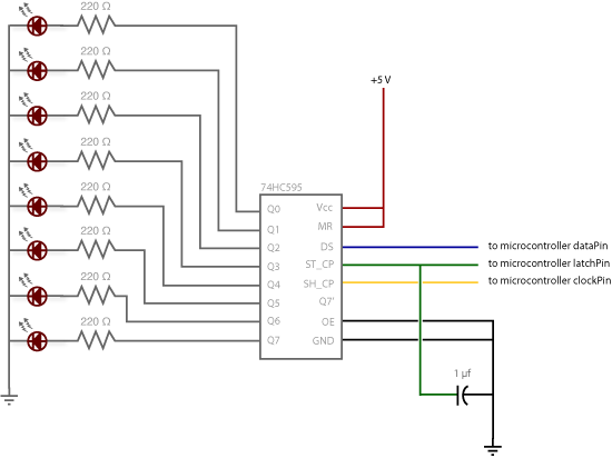
Make the following connections: GND (pin 8) to ground, Vcc (pin 16) to 5V, OE (pin 13) to ground, MR (pin 10) to 5V. This setup makes all of the output pins active and addressable at all times. The...
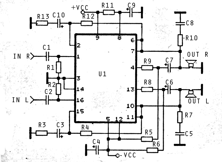
The audio amplifier circuit is highly suitable for home use, particularly with subwoofer or woofer speakers. Commonly referred to as a home amplifier, these audio amplifiers are based on integrated circuits (ICs), specifically the STK series, which includes models...
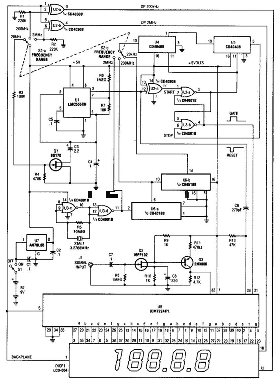
This is a schematic and block diagram of a 2-MHz frequency counter. It utilizes an LSI counter/display driver, an LCD readout, and several logic chips for timebase and timing pulse circuitry. Q2 and Q3 serve as a signal (input)...