
maintenance sanwa yx 360tr schematic diagram
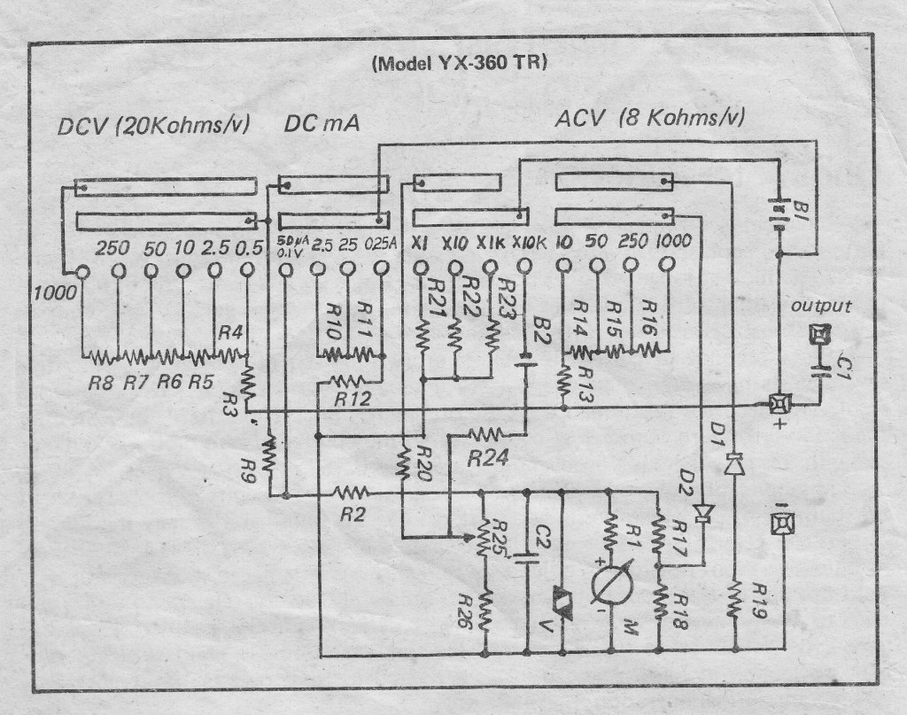
The schematic diagram of an Analog Multitester typically features a variety of components arranged to perform measurements of voltage, current, and resistance. The core of the circuit often includes a galvanometer, which is a sensitive ammeter that indicates the flow of current. This component is usually accompanied by a series of resistors that help to scale the measurements appropriately for different ranges.
In addition to the galvanometer, the circuit may include a switch for selecting between different measurement modes, such as DC voltage, AC voltage, and resistance. This switch is essential for directing the input signal to the correct part of the circuit. Resistors and capacitors are also employed to filter and stabilize the readings, ensuring accuracy in the measurements.
The design may incorporate a battery or power supply circuit, which provides the necessary voltage for operation. A protective fuse is often included to prevent damage to the multimeter in the event of an overload condition.
Furthermore, the output of the circuit is typically displayed on an analog scale, which allows users to read the measurements visually. The layout of the components in the schematic is crucial for ensuring that the multimeter operates effectively and safely, allowing for reliable testing and diagnostics in various electronic applications.
This schematic diagram is valuable for both hobbyists and professionals in the field of electronics, providing insight into the operation and construction of Analog Multitesters across different brands.For those who are looking for a copy of the schematic diagram on this type of Analog Multitester and other brand using the same circuit diagram.. 🔗 External reference
Related Circuits

The circuit consists of a radio remote lighting switch utilizing RCM1 type radio-controlled remote control transmitter and receiver components. It features the RCM1A/B component, which facilitates the remote control functionality. Additionally, the design incorporates a remote control transmitter and...
The fundamental concept involves a high-frequency, high-voltage, low-current signal that is rectified and subsequently utilized to charge a bank of high-value capacitors. These capacitors are then discharged in pulse mode for brief intervals, specifically in the nanosecond range, through...
RF Wireless Data Transfer communication circuit diagram. A wireless communication interface was implemented to facilitate data transfer from one point to another using RF technology. The RF Wireless Data Transfer communication circuit utilizes radio frequency (RF) technology to establish a...
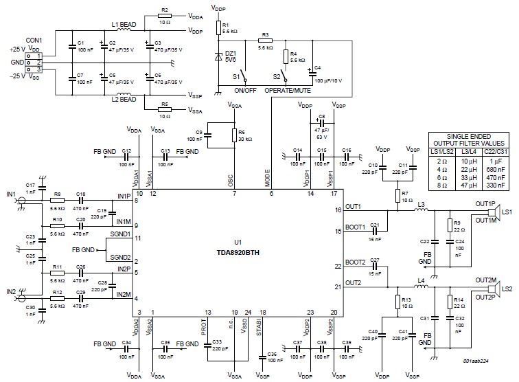
This high-power Class D audio amplifier electronic project utilizes the TDA8920BTH audio power amplifier integrated circuit (IC). This power amplifier IC is characterized by its high efficiency and low heat dissipation, delivering significant output power. The typical output power...
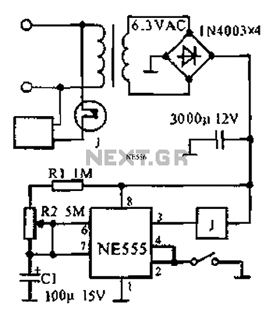
The provided information indicates that when the power supply operates between 0 to 1 hour, an AC circuit diagram is established using a 555 timer configured as a one-hour timer. The relay utilized is a J 212 IRC MR312C...
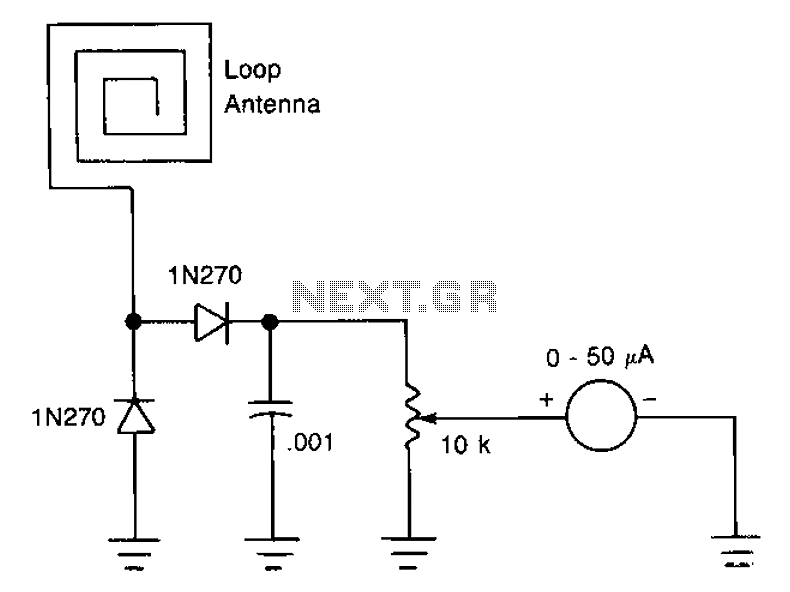
The antenna consists of approximately 20 cm of insulation made from strands, which are glued together inside a small plastic box. An RF current is processed through two diode rectifiers, and a 10k potentiometer is connected to the pin...