
Handheld Laser Circuit

The circuit utilizes the TOLD9200 laser diode, which is known for its efficiency and capability to emit coherent light. The touch switch, comprising transistors Q3 and Q2 along with switch SI, enables user interaction by allowing the laser to be activated or deactivated through a simple touch, providing a user-friendly interface.
The RF pickup coil, L1, plays a crucial role in energy harvesting. By employing 10 turns of #18 gauge wire, the coil is optimized for capturing electromagnetic energy generated by an RF charger. The Y-shaped diameter of the coil enhances its inductance and efficiency, making it suitable for wireless energy transfer applications.
In the schematic, the power supply to the laser diode is controlled by the touch switch components. When the user touches the switch, a small current flows through Q2, which activates Q3, allowing current to flow to the laser diode. The operation of the laser diode can be adjusted based on the input signal from the touch switch, providing flexibility in its application.
This circuit can be applied in various applications, such as portable laser devices, where efficient power management and ease of use are essential. The integration of RF energy harvesting allows for sustainable operation, reducing the need for traditional battery replacements and enabling the device to function in a more eco-friendly manner. A laser diode TOLD9200 (Toshiba) is used as a source of laser light. Q3, Q2, and SI form a touch switch to control the.laser. LI is an RF pickup coil to pick up energy from an RF-type battery charger. It is 10 turns of #18 wire on a Y diameter. 🔗 External reference
Related Circuits
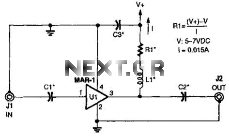
The low-cost Mini-Circuits MAR-X series of chips provides a significant advantage for RF builders, featuring inherent 50-ohm input and output impedances essential for RF systems. An MAR-1-based receiver/scanner preamplifier is illustrated. Capacitors Ci and C2 are chip capacitors, with...
To configure the amplifier, set resistor R1 to its maximum value and resistor R12 to zero. After this adjustment, power on the amplifier. Adjust R1 until the measured output offset is between 30 mV and 100 mV. Once this...
This project was a final assignment for an optics class (EE 134) at Stanford University. It was an open-ended task aimed at creating a fully functioning laser microphone. The class focused on demonstrating optics and photonics in the laboratory...

This 1000-watt power inverter circuit diagram is based on the MOSFET RF50N06. For increased power output, additional MOSFETs can be paralleled with the RF50N06. These MOSFETs are rated for 60 volts and 50 amps. It is essential to connect...

The accumulator charger circuit must provide a voltage that matches the specifications of the batteries being charged. For a 12-volt accumulator, the output voltage should not exceed 12 volts, nor should it fall significantly below this threshold. Failure to...
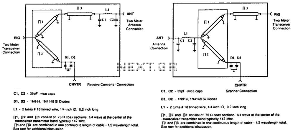
A pair of diodes and a quarter-wave transmission line are utilized as an automatic TR switch. D1 and D2 conduct during transmit periods, short-circuiting the scanner input. In this mode, the quarter-wave line appears as an open circuit. In...