
Hardware design overview
It sacrifices a lot of the features you`d look for in a full-scale development board to achieve our primary goals: You can get your own assembled Open Logic Sniffer at Seeed Studio for $45, including worldwide shipping. Continue reading about the design and collaboration below. SUMP is an open source Java logic analyzer client by Michael Poppitz. It consists of two parts, a VHDL logic capture engine for FPGAs, and a Java logic analyzer client. The latest development version of the SUMP client is available from SourceForge. net. SUMP is a sampling logic analyzer. It reads the state of the input pins and stores the samples in internal ram. It then dumps the samples back to the computer client for analysis. The number of samples possible is limited by the RAM in the FPGA. We like SUMP because it`s the best developed open source logic analyzer toolchain currently available.
It has lots of professional features like multi-stage triggers, configurable pre-roll, external trigger and clock sync, and a few protocol analyzers (I2C, UART). It`s open source, so the potential to add cool new features is limited only by your imagination and coding skills.
SUMP is typically ported to a general-purpose FPGA development board. We took a different approach and designed hardware specifically for SUMP, while constraining costs wherever possible. Professional logic analyzers have tons of channels and super high speeds. We`re not trying to make a low cost DIY version of these tools, the OLS isn`t an alternative to these types of tools if you need to sniff 100MHz+ signals and have huge sample sizes.
Being an engineer`s tool, there are plenty of DIY logic analyzer designs. Parallel port based logic analyzers used to be all the rage, but with parallel ports and direct interrupt access disappearing from systems, these are just historical curiosities. Another type of DIY logic analyzer is a microcontroller-based device. There are several with custom interfaces like the PIC Logix, Scanalogic, and AVR Logic Analyzer. The Bus Pirate works with SUMP. Microcontroller analyzers all have one thing in common: they`re really slow, usually sub-megahertz. USB IO chip-based hobby logic analyzers are currently popular. We`ve always been fans of the Saleae Logic, the USBee is similar. These devices are just a USB IO chip like a CY7C68013A-56PVXC, with all trigger and processing logic done in software on a computer.
The hardware part is just a datalogger. The top sampling speed is usually around 24Msps (24MHz), if the conditions on your USB bus are just right. They can take `unlimited` samples because everything is stored on the computer. Current models tend to be 8 channels, more channels would reduce the maximum speed proportionately. These are commercial products with highly polished user interfaces, we don`t know of any that are open source.
The Open Logic Sniffer sits somewhere between hobby analyzers and professional analyzers. The OLS samples up to 200Msps, regardless of the USB bus traffic, and has true hardware triggers. The OLS has twice as many buffered channels as most hobby USB analyzers, and four times more channels overall. The major difference is that the OLS has a limited number of samples, while the hobby USB analyzers can theoretically take infinite samples.
Most of our debugging is done with the first few hundred samples, so this feature isn`t usually important to our work, your situation may be different. Future versions of the OLS will definitely have more sample storage, and we can work an infinite sampling mode into a future firmware update too.
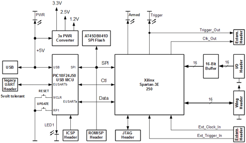
Click for a full size circuit diagram [PNG]. This circuit diagram, maintained by Uwe Bannow, shows the basic elements of the Open Logic Sniffer hardware. The FPGA captures logic samples from 32 input pins into internal RAM. The samples are dumped out a serial port for analysis on a computer. The open source SUMP logic analyzer client is used to capture and visualize the samples. The FPGA only communicates over a serial port, so we used a USB microcontroller to convert the serial IO to a USB virtual serial port.
The entire chain is upgradable through the USB connection. The microcontroller can program updated logic analyzer designs into the SPI flash data chip, and the microcontroller can also be updated from its USB bootloader. We chose a USB microcontroller over a dedicated USB interface chip. A low pincount PIC was cheaper than most other USB bridge options. It`s USB 2. 0 compliant, and can transfer data at up to 12Mbps. We`re using it with the completely open virtual serial port CDC interface, so it will work on almost any platform without proprietary drivers.
The PIC can also implement other USB transfer protocols with a firmware update, faster connection methods can be supported when someone adds support for them to the SUMP client software. Currently the SUMP FPGA design only transfers data over a 115200bps serial UART, the speed between the USB PIC and the computer isn`t a bottleneck.
We routed several extra connections between the PIC and FPGA to implement a high-speed SPI interface in the future. The speed increase of an SPI interface can be supported in the SUMP client just by adding higher serial port speed settings.
With so much to accomplish already, major modifications to the client to work with untested hardware and custom drivers didn`t seem appealing. Not if the project were ever going to get finished. The PIC seemed like the best route for the first version. Click for a large image of the schematic [PNG]. The schematic is divided into a microcontroller part [PNG] and a FPGA part [PNG]. These sections are where Ian and Jack initially split the design work. We used the freeware version of Cadsoft Eagle to make the circuit and PCB. Download the latest files from the Gadget Factory project page. A Xilinx Spartan 3E field programmable gate array ( FPGA ) is the central component of the logic analyzer.
The FPGA samples data from 16 buffered and 16 unbuffered IO pins, and stores the samples in internal RAM. The samples are later dumped out a serial UART to the PIC, and from the PIC to a computer via USB. . 🔗 External reference
Related Circuits
Voltage measurement is a fundamental aspect of electronic technology today, with increasing demands for accuracy and functionality in instruments. This is particularly critical when measuring signals with significant phase differences, as it is essential to ensure the accuracy of...
Field bus technology and intelligent instrument technology are currently two of the most rapidly evolving technologies in automation and control. In the realm of field bus technology, the CAN bus has established itself as a relatively fast communication standard...
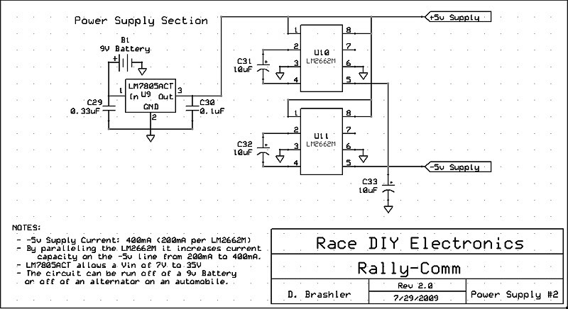
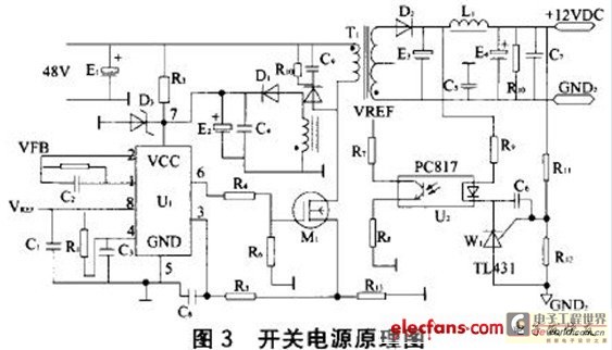
This circuit utilizes the LM2662M integrated circuit from National Semiconductor, which serves as a direct replacement for the MAX1044 but in a smaller surface mount package. Additionally, the main voltage regulator has been upgraded to the LM7805ACT. This circuit...
The motor vehicle currently represents a no-emission automotive solution, serving as a green means of transportation that is expected to significantly impact human society in the 21st century. The direct-flow brushless electric machine has emerged as a leading technology...
A simple ultrasonic parking sonar electronic project can be designed using this schematic circuit. This ultrasonic parking sonar project features an adjustable detection range from 5 cm to 1.5 meters and a detection angle of 5 degrees. The circuit...
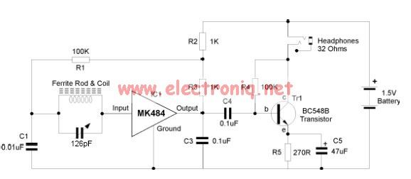
The MK484 AM radio circuit offers a comprehensive solution featuring an RF amplifier, detection, and an automatic gain control (AGC) circuit. It requires only a few external components to achieve high-quality AM tuning. The circuit has an input impedance...