
High operating voltage regulator circuit diagram
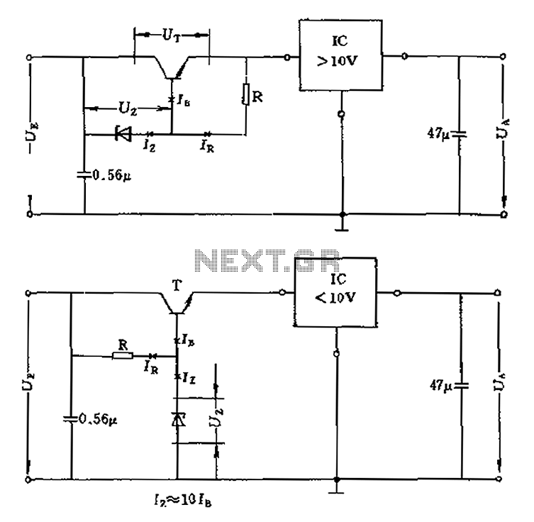
The voltage regulation circuit operates based on the principles of transistor behavior and Zener diode regulation. The equation Ue = Ut + Ur + Ua outlines the relationship between the input voltage (Ue), the transistor voltage drop (Ut), the reference voltage (Ur), and the output voltage (Ua). The maximum output voltage (Ua) is influenced by the transistor voltage (Ut), which is a critical parameter for ensuring the circuit's efficiency.
In the design of this voltage regulator, the Zener diode plays a pivotal role. The Zener voltage (Uz) must be selected to be at least 4V higher than the desired output voltage (Ua) to ensure stable operation. This margin allows for variations in load and input voltage while maintaining a constant output. The resistor R is selected based on the current requirements, which must satisfy the boundary conditions of the circuit. The relationship Ir = Iz + Ib indicates that the current flowing through the resistor R (Ir) must equal the sum of the Zener current (Iz) and the base current (Ib) of the transistor.
When designing the circuit for a lower input voltage, such as Ue = 5V, careful consideration must be given to the components selected to ensure that they can handle the operational constraints. The integrated circuit utilized in this design is optimized for higher operating voltages, thus enabling it to function effectively even when the input voltage is significantly lower.
In summary, the design of the voltage regulator requires meticulous selection of the Zener voltage and resistor values to achieve the desired output voltage while ensuring stability and performance across varying conditions. Proper understanding of the relationships between the input voltage, transistor characteristics, and Zener diode behavior is essential for effective circuit design. By the voltage equation Ue Ut + Ur + Ua shows that the size of the transistor voltage Ut will determine the maximum output voltage Ua. At the same time there should be Ur 2V. U t voltage regulator voltage value depends on the choice of Uz. Figure a resistor R is selected to satisfy the boundary conditions Ir Iz Ib formula or principle + Ir F10 Ibs. This integrated circuit is adapted to have a higher operating voltage of the occasion, at a lower voltage, for example Ue 5V, the circuit should be used in Figure b.
Zener voltage higher than the output voltage of at least Ua4V. Resistor R selection circuit with a.
Related Circuits
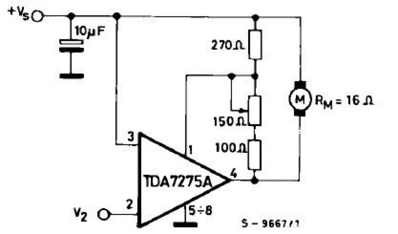
The TDA7275A linear integrated circuit, housed in a minidip plastic package, can be utilized to design a straightforward speed regulator electronic project suitable for regulating the speed of small DC motors. The TDA7275A DC speed controller project is specifically...
The diagram illustrates a series connection of cell diode capacitors, each rated for an increasing voltage of 300 V. This configuration generates a high DC voltage supply of 40 kV, which can be utilized for various experimental applications. With...
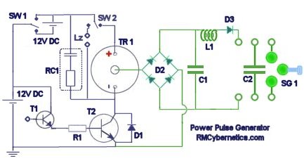
This picture and schematic were intended for posting on my Watson's blog, but it did not get published. The circuit schematic in question likely includes various electronic components arranged to perform a specific function. Typically, such schematics are used to...
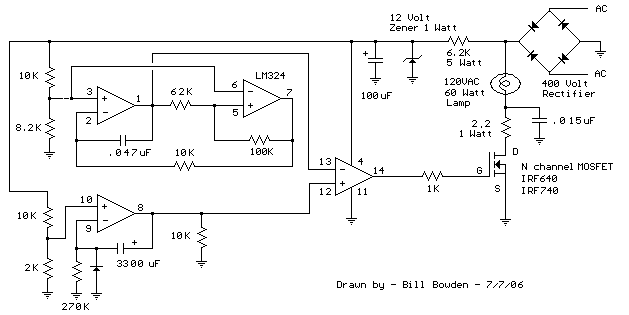
This circuit gradually illuminates a 120VAC lamp over an approximate 20-minute period. A bridge rectifier converts the AC voltage to 120V DC, supplying power to the MOSFET and the 60-watt lamp. A 6.2K, 5-watt resistor along with a Zener...
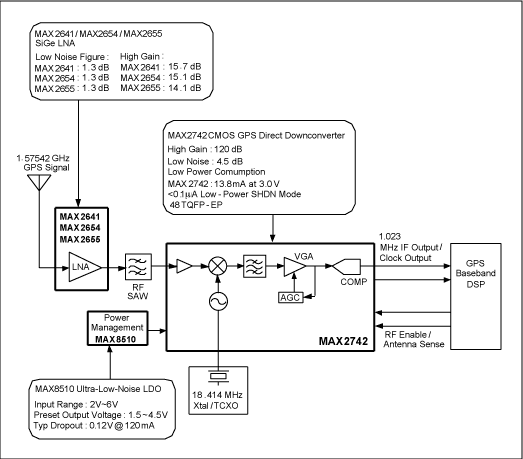
The following circuit illustrates the RF block diagram of a GPS receiver. This circuit is based on the MAX2742 integrated circuit. Features include a complete GPS receiver functionality. The GPS receiver RF block diagram utilizing the MAX2742 IC encompasses several...

Lithium-based (Li+) batteries are increasingly used in portable devices due to their favorable characteristics. However, they are often in limited supply, leading to long lead times unless a preferred-customer status is established with manufacturers. Consequently, a backup alternative to...