
High-voltage power pulse circuit

The circuit operates by charging capacitor C1 to a voltage HV through resistor R1 and diode D1 when the HV supply is applied. A 0-V control signal keeps PowerFET Q1 in the off state. When a 5-V signal is applied to the control input, it drives the driver IC2, which outputs a 12-V signal to the gate of PowerFET Q1, allowing it to conduct. Consequently, the output of the circuit reaches HV volts as the negative terminal of C1 is grounded. The pulse concludes when the control signal returns to 0 V. The useful pulse length is constrained by the voltage drop during the pulse (resulting from C1 discharging) and the 100-µs/64-A safe limit of the PowerFET. For the specified values, the circuit experiences a 10 V drop for a 1-µs, 10-A pulse.
Short-circuit and overload protection is managed through R1. As the output current increases, the effective gate-source voltage of the PowerFET decreases, thereby increasing the FET resistance. Given a 0.1-Ω value, the output current is limited to 50 A. In a short-circuit scenario, capacitor C1 can be safely discharged through the PowerFET. Diode D1 mitigates reverse voltages induced by inductive loads. When not in operation, resistor R14 discharges C1 for safety.
Circuit layout is critical; a ground plane is essential to minimize inductance. C1 must be a low-inductance pulse capacitor, and the layout for FET driver IC2 should also prioritize low inductance and effective decoupling. Leading-edge gate currents can reach up to 2 A to charge the FET input capacitance. Resistors R1 and R2 should consist of at least ten paralleled discrete components to achieve low series inductance. Resistors R4 and capacitor C3 are utilized to compensate for any remaining inductance in R2 (the value of C3 can be adjusted accordingly). Components C2, R5, R6, and R7 create a snubber network to protect the FET from voltage spikes. The specified values for voltage and current monitoring are calibrated for a 50-Ω load. Higher currents can be achieved by duplicating the IC2-Q1-R1 stage and connecting them in parallel, with R1 serving to balance the current across each stage. A 100-A pulser has been successfully constructed using this method.Fast rise-time high-voltage pulses have many uses ranging from EMC testing to device characterization. The simple, low-cost circuit described here deals with the latter. It`s able to generate 0- to 1000-V pulses with currents up to 50 A, and a rise time of 100 ns for 800 V/30 A.
The output can withstand short circuits, and capacitive and inductive loads. Pulse length and repetition rate are determined by an optically isolated TTL-input signal. Commercial equipment like pulse/function generators or a PC can be connected to this input. The pulse`s amplitude is set by the HV supply; a low-cost photomultiplier-type supply (0, 5. 5 mA) can be used when repetition rates are below 20 Hz. The circuit operates as follows: when applying the HV supply, C1 is charged up to a voltage HV via R1 and D1 ( see the figure ). A 0-V control signal keeps the PowerFET Q1 in the off state. A 5-V signal on the control input operates the driver IC2, from which a 12-V signal is presented on the gate of the PowerFET Q1, bringing it into conductance.
The output of the circuit becomes ’HV volts as the negative terminal of C1 is now grounded. The pulse ends by making the control signal 0 V. Useful pulse length is limited by he voltage drop during the pulse (caused by discharging C1) and by the 100- µs/64-A save limit of the PowerFET. For the values shown, the circuit voltage drop is 10 V for a 1- µs, 10-A pulse. The short-circuit and overload protection is based on R1. When the output current is rising, the effective gate-source voltage of the Power-FET diminishes, enlarging the FET resistance.
With the given 0. 1- © value, the output current is limited to 50 A. In a short-circuit situation, capacitor C1 can be fully (and safely) discharged in the PowerFET. Reverse voltages caused by inductive loads are eliminated by D1. When the circuit isn`t operating, R14 discharges C1 for safety reasons. Circuit layout is very important ”a groundplane is needed to keep inductance low. C1 must be a low-inductance pulse capacitor. Even the FET driver IC2 needs a low-inductance layout and decoupling. During the leading-edge gate currents, up to 2 A are needed to charge the FET input capacitance. Resistors R1 and R2 have to be made of at least 10 paralleled discretes to get a low series inductance. R4 and C3 compensate for the remaining inductance in R2 (the value of C3 can be changed for this). C2, R5, R6, and R7 form a snubber network to protect the FET against voltage spikes. The values for the voltage and current monitor levels are given for a 50- © load. Higher currents can be obtained by duplicating the IC2-Q1-R1 stage and connecting them in parallel. R1 helps to equalize the current for each stage. A 100-A pulser has been successfully built in this manner. 🔗 External reference
Related Circuits
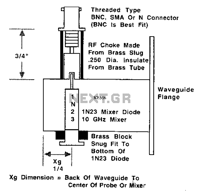
This is a 10 GHz frequency amateur radio waveguide detector. The 10 GHz amateur radio waveguide detector is designed to operate within the microwave frequency range, specifically targeting the 10 GHz band commonly used in various amateur radio applications. The...
A dual benefit for battery-powered portable devices is provided by Class D audio amplifiers. They produce much less power dissipation than their linear counterparts. Class D audio amplifiers, also known as switching amplifiers, are designed to achieve high efficiency and...
The power is all in the timed switching process. There are two main principles I use of switching the radiant energy the John Bedini way. First, the SG/SSG, Icehouse unidirectional circuit or John Bedini Monopole with the School Girl...
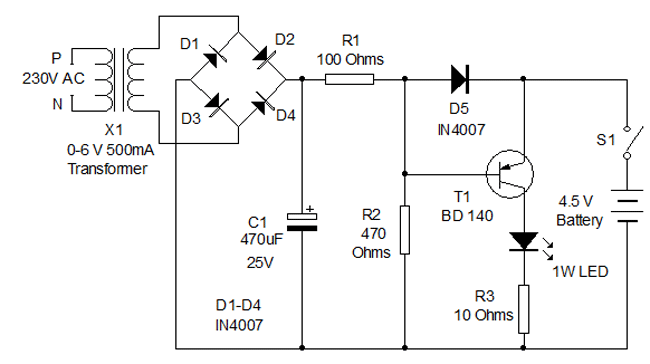
Circuit diagram for a mini emergency lamp. This mini emergency lamp activates during power failures to provide cool white light in the room. It utilizes a 1-watt white LED to deliver adequate illumination. The circuit for the mini emergency lamp...
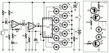
The following circuit illustrates a Dancing LEDs electronic circuit diagram. This circuit is based on the LM358 integrated circuit. Features: IC1A amplifies the signal. The Dancing LEDs circuit utilizes the LM358 operational amplifier to create a visually appealing light display....
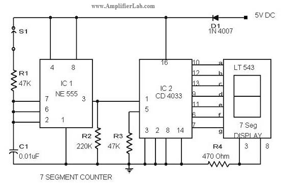
The circuit diagram of a 7-segment counter circuit has been published here. This circuit consists of the counter IC CD4033 as its central component. The 7-segment counter circuit utilizing the CD4033 integrated circuit (IC) is designed to display decimal digits...
Warning: include(partials/cookie-banner.php): Failed to open stream: Permission denied in /var/www/html/nextgr/view-circuit.php on line 713
Warning: include(): Failed opening 'partials/cookie-banner.php' for inclusion (include_path='.:/usr/share/php') in /var/www/html/nextgr/view-circuit.php on line 713