
How to design A class amplifier

1. Id - It is a silicon NPN general-purpose type.
2. Pd - 0.5W meaning it is capable of dissipating 500mW.
3. Vce - 40V meaning do not use it above 20V (preferably less) d.c. supply.
4. Ic - 0.8A meaning the maximum collector current allowed is 800 mA.
5. Hfe - 100 @ Ic of 150 mA, indicating an amplification factor of 100.
6. Ft - 300 MHz meaning that by the time the frequency reaches 300 MHz, the amplification factor has dropped off to 1.
7. Case - TO-18 type package (not always).
Rule 1: Do not always believe all of those specs. Most specs are the conservative limits, but important items such as the gain Hfe vary widely. On a bunch of these transistors, gain figures ranging from 60 to 170 have been measured. Always use your transistor well under the published specifications.
The 2N2222A transistor features three terminals: the BASE (B), EMITTER (E), and COLLECTOR (C). The schematic symbol for a transistor indicates its configuration, with an arrow pointing toward the emitter symbol, signifying that it is an NPN type. In contrast, a PNP type has the arrow pointing in the opposite direction.
When the base terminal is open, a small current flowing into the base will result in a significantly larger current flowing through the collector, a property that defines the transistor as a current amplifier.
Rule 2: Do not take the EBC connections or leads of transistors for granted. Different manufacturers may have different pinouts, even for the same type. Always double-check the specifications.
In a transistor amplifier, two distinct sets of conditions exist: the direct current (d.c.) conditions and the alternating current (a.c.) or radio frequency (r.f.) conditions. The efficiency of 50% is often an idealized expectation; in practice, achieving this efficiency is rare. The class A amplifier design is favored at low signal levels and amplifications, where losses due to inefficiency are less significant compared to the pursuit of fidelity and linearity in radio frequency applications.Feedback - This is where part of the output signal is fedback to the input BUT 180o out-of-phase (i.e. partially cancels the input). If it were in-phase feedback then we would have an oscillator - which in this case we definitely do not want.
Fidelity - This means many things to many people but to us it means the output must be an exact replica of the input but only magnified or amplified. Efficiency - The theoretical limit to this amplifier's efficiency is 50%, meaning for every watt of output we will use up at least 2 watts of d.c.
power input in to the amplifier. Depending upon the application this may or may not be significant. If we have a large power transformer available to us and power, literally to burn, who cares?. On the other hand if miniaturisation were the keyword and precious battery supply is the only power source available thennnnnn! that's another matter. For this I have selected a very popular, cheap and extremely versatile transistor and reproduced it's pertinent specifications below.
This is the 2N2222A. There are many other similar types available. 1. Id - It is a silicon NPN general purpose type. 2. Pd - 0.5W Meaning it is capable of dissipating 500mW. 3. Vce - 40V Meaning do not use it above 20V (preferably less) d.c. supply. 4. Ic - 0.8A Meaning the maximum collector current allowed is 800 mA. 5. Hfe - 100 @ Ic of 150 mA This means it has an amplification factor of 100. 6. Ft - 300 Mhz this means that by the time the frequency reaches 300 Mhz the amplification factor has dropped off to 1. 7. Case - TO-18 type package (not always). Rule 1: Do not always believe all of those specs. Most specs are the conservative limits but important items such as the gain Hfe, varies widely. On a bunch of these transistors I have measured gain figures ranging from 60 to 170. Always use your transistor well under the published specifications. O.K. we have our little 2N2222A sitting on the bench in front of us. What good is that? Alright let's look at it (or even a similar type). It has three legs or leads coming out of it. Look at figure 1. One is called BASE (B), another is called EMITTER (E) and the other is called the COLLECTOR (C). A transistor schematic symbol looks like this: Figure 1. You will notice an arrow pointing toward the emitter symbol. This indicates our transistor is an NPN type. There is also a PNP type where the arrow points in the opposite direction. That is a fairly specialised type of transistor and we will not bother with it any further here. With the above transistor, if the base is open, then a small amount of current flowing into the base will lead to a much larger current flow in the collector.
The ratio is the gain of the particular transistor. Hence a transistor is known as a current amplifier. Rule 2: Do not take the EBC connections or leads of transistors for granted. Different manufacturers have different pin outs, even for the same type. Always double check!!!!. In a transistor amplifier we have two totally different sets of conditions. One set are the d.c. conditions and the other set is the a.c. or r.f. conditions. Both are depicted here in Figure 2: Most experts will agree with me when I say you will only see this 50% efficiency in your dreams. So why use class A?. At low levels of signal and amplification, the losses through inefficiency are not significant and are far outweighed by the goal of fidelity or in the r.f.
game, linearity, i.e. a linear amplifier. 🔗 External reference
Related Circuits
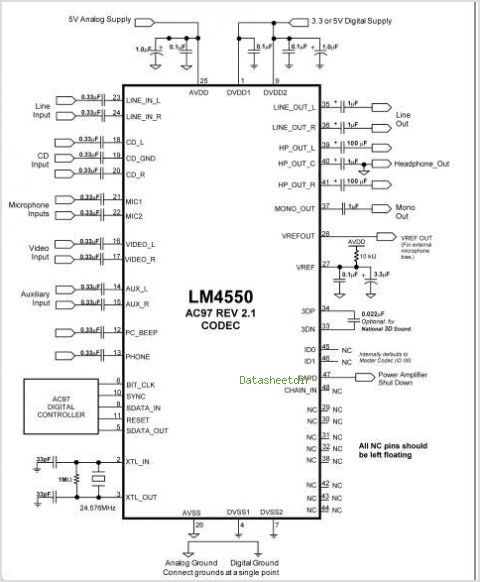
The LM4610 is a DC-controlled tone (bass/treble), volume, and balance circuit designed for stereo applications in car radios, televisions, and audio systems. It also incorporates National's 3D-Sound circuitry, which can be adjusted externally using a simple RC network. An...
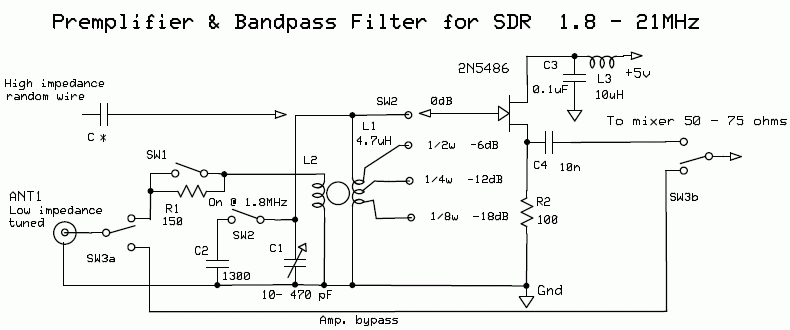
The Software Defined Radio (SDR) hardware, in its most basic configuration, includes a wideband switched balanced mixer and a low noise LF amplifier. This straightforward hardware demonstrates remarkable sensitivity and linearity, making it suitable for both testing and regular...

A photodiode can be utilized for high-speed digital transmission; however, it is necessary to provide a high-speed signal conditioner for this purpose. The amplifier circuit... A photodiode is a semiconductor device that converts light into electrical current. In high-speed digital...
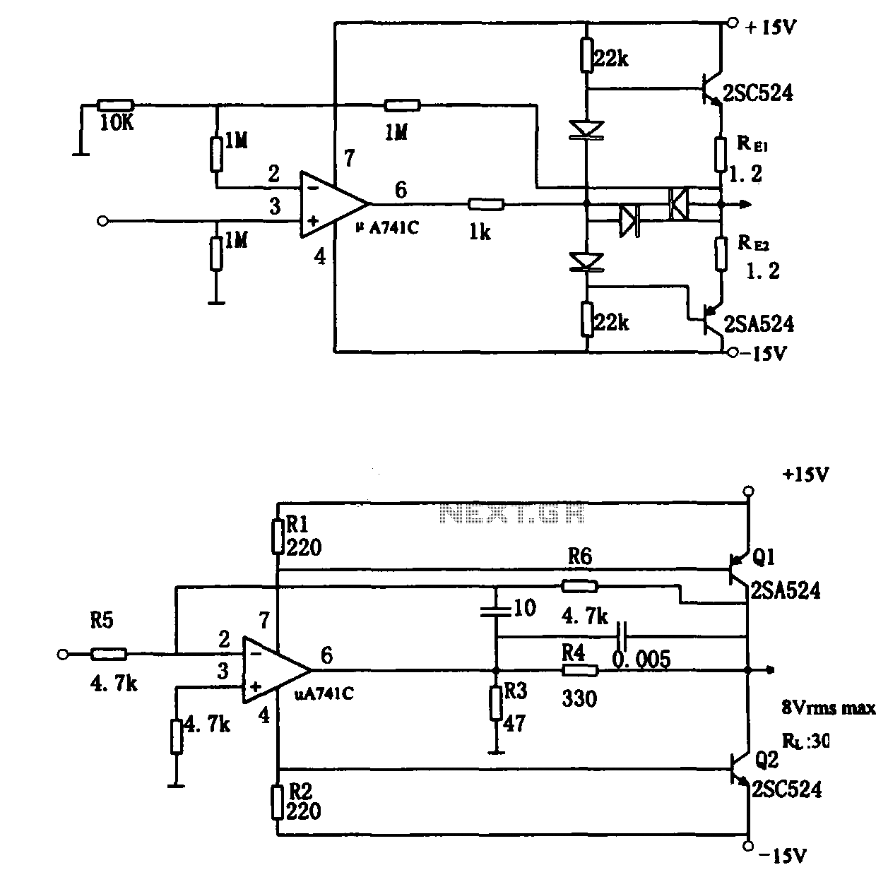
The direct coupling audio power amplifier utilizes an integrated operational amplifier. There are typically two practical configurations. The first configuration, depicted in (a), features a circuit structure that includes the output of the operational amplifier and a complementary symmetry...

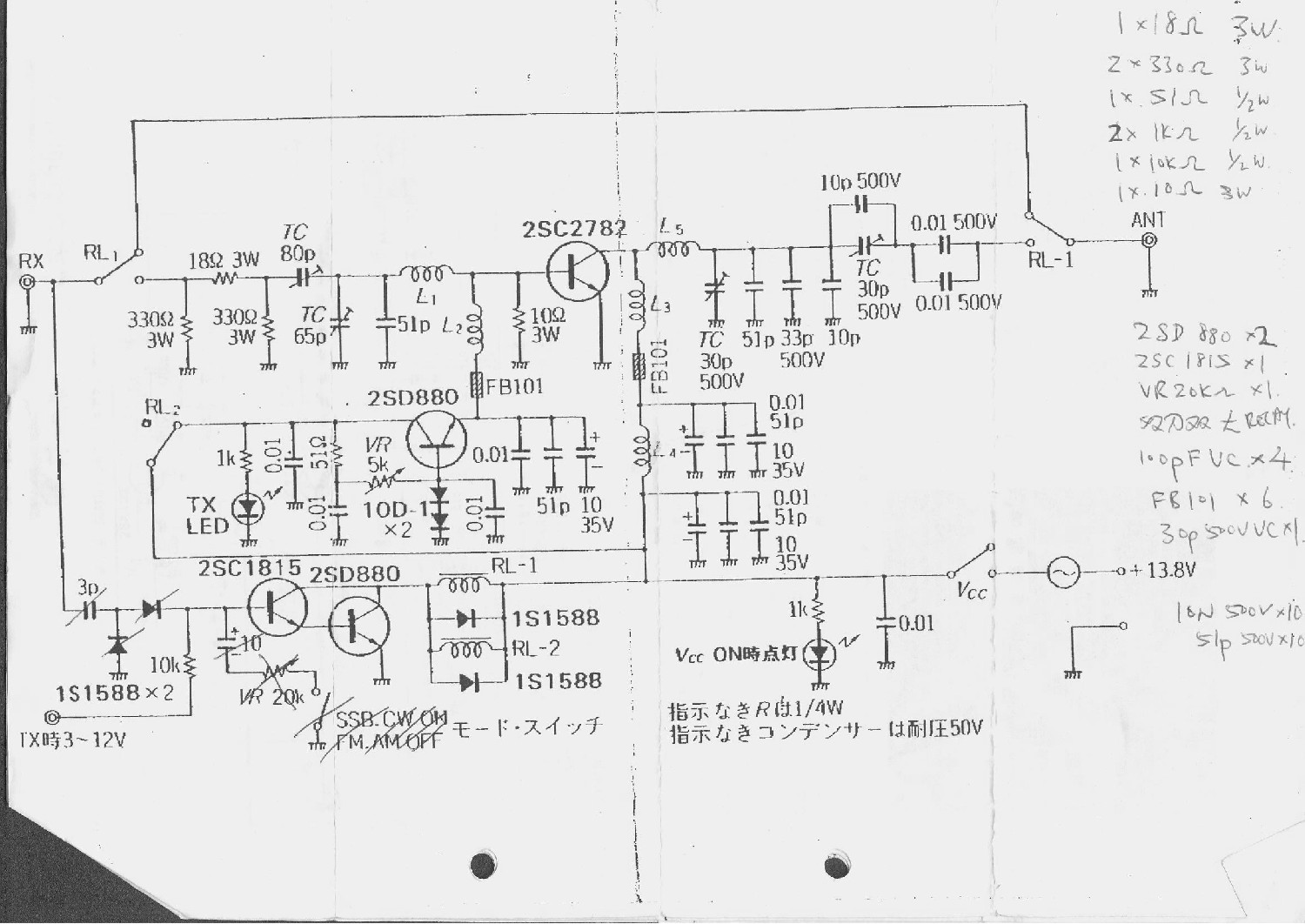
This is a preamplifier circuit and switching schematic for the Marantz Model 33. The Marantz Model 33 preamplifier circuit is designed to amplify low-level audio signals from various sources before sending them to a power amplifier. The schematic typically includes...
This is a 6-meter band transmitter RF power amplifier designed for 50 MHz operation, delivering an output power of 100 watts. It is intended for use with the FT-736R transceiver and is driven by a 10-watt signal for 6-meter...