
Input Impedance Booster II
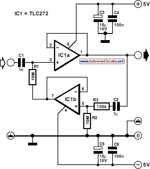
In the context of this AC-coupled operational amplifier circuit, the input resistance plays a critical role in determining the overall performance and stability of the system. The use of CMOS technology is beneficial due to its high input impedance, which minimizes loading effects on the preceding stage. The bootstrap technique is particularly useful for applications requiring extremely high input resistance, as it allows for the effective enhancement of the impedance seen at the input without introducing significant noise or distortion.
The configuration of resistor R1 is pivotal in establishing the desired DC operating point, ensuring that the operational amplifier functions within its optimal range. The feedback network, comprising capacitors and resistors, is designed to facilitate proper AC signal handling while maintaining the DC biasing conditions. The careful selection of resistor values is essential for achieving the target input resistance; hence, adherence to the specified limits on R3 and R2 is critical to prevent instability.
In practical applications, such circuits can be utilized in various signal processing tasks, including sensor interfacing, audio processing, and instrumentation, where high input resistance is paramount. The design considerations outlined ensure that the circuit remains stable and performs effectively across a range of operating conditions.The input resistance of a. c. -coupled op amp circuits depends almost entirely on the resistance with which the d. c. setting is determined. If CMOS op amps are used, the input resistance is normally high, currently up to 10 M. If a higher value is needed, a bootstrap circuit may be used. This enables the input resistance to be boosted artificiall y to a very high value, indeed In the circuit shown in the diagram, resistor R1 sets the d. c. point for IC1a. The terminal of the resistor linked to pin 7 of IC1 would normally be at earth potential, so that the input impedance would be 10 M. Connecting the other terminal of the resistor to earth via IC1a and network C2-R3-R2 as far as d. c. is concerned results in the requisite d. c. setting of the op amp. As far as alternating voltages are concerned, the input signal is fed back so that only a tiny alternating current flows through R1.
Therefore, Rin=R1[(R2+R3)/R3]. With resistor values as specified, Rin is about 1 G. One aspect must be borne in mind: the numerical value of (R2+R3)/R3 must not exceed 0. 99. This means that the value of R3 cannot be less than 100 k if the value of R2 is 10 M. If these conditions are not met, the circuit will become unstable. 🔗 External reference
Related Circuits
This schematic represents a cable TV signal booster amplifier circuit designed to enhance the signal strength of a cable TV system. It is recommended to use 75 Ohm coaxial cables for both the input and output connections, and the...
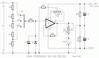
The MOSFET input of the CA3140 is ideally suited for use in a high impedance DC voltmeter. The range selector is controlled by switch S1. The input impedance is limited to 10M by the resistors in the voltage divider,...
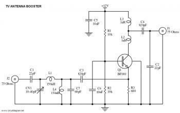
This is a straightforward circuit for a UHF band TV antenna booster that provides a gain of 15 dB. This low-cost antenna booster is simple and easy to construct. The UHF band TV antenna booster circuit is designed to enhance...
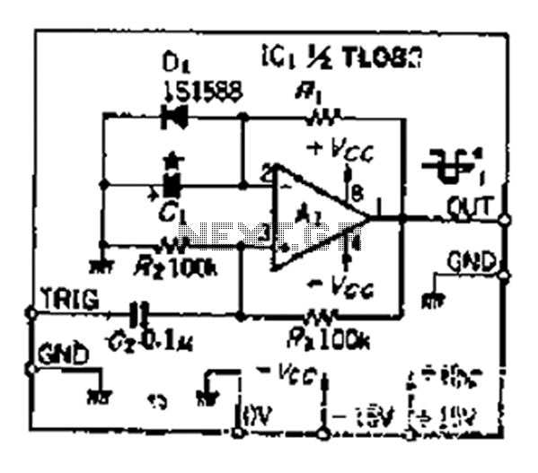
Although people believe that using a timer with an operational amplifier (op-amp) does not yield significant results, it can still be advantageous in certain scenarios. In environments with high noise levels, the application retains its benefits. When the phase...
This circuit takes two separate line-level stereo (L & R) signals and combines them into one stereo (L & R) output, thus avoiding the need to switch between them. The circuit is designed to facilitate the merging of two independent...
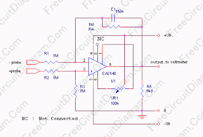
In some cases, a cogwheel input is necessary for voltage measurement. By utilizing a single operational amplifier, an adapter can be created to accommodate a differential input for a ground-referenced voltmeter. It is recommended to use 1% tolerance metal...