
Input programming activity
The input for the potentiometer is managed digitally through assembly code, which is structured for compatibility with the MPLAB development environment and the specific processor, in this case, the PIC16F676. The configuration settings include disabling the comparator, turning off the brown-out reset, and enabling the power-up timer while disabling the watchdog timer. The hardware equates define the pin assignments for the switch and potentiometer on Port A. The program memory begins with an oscillator calibration routine, ensuring that the oscillator operates within specified parameters. The initialization process involves configuring the ports for digital input and output, ensuring that the system is prepared for interaction with the defined input circuits. The assembly code effectively sets up the microcontroller to handle the various input signals, allowing for the digital processing of signals from the potentiometer and other input devices. This systematic approach to input handling is crucial for the reliable operation of the circuit board in various applications.Now, let`s re-examine the function of the TRIS registers. The TRISA and TRISB registers control the direction of data transfer on each pin of Port A and Port B, respectively. The easy way to remember the TRIS register settings is to match the numbers 0 and 1 to the letters O and I: The CHRP circuit board includes a number of input circuits, such a
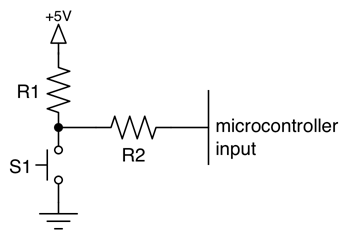
s pushbutton switches, phototransistors (light sensors), and a potentiometer (position sensor). All of these inputs operate in a similar, though slightly different way. Examine the switch input schematic diagram, below: The switch (S1) and pull-up resistor (R1) form a series circuit, also known as a voltage divider. The microcontroller input is connected to the output at the mid-point of the voltage divider, and senses the electrical potential across the switch.
Since any microcontroller pins configured as inputs have a high impedance, they will just sense the externally applied voltage but won`t conduct any appreciable current themselves. This essentially means that the effect of the series resistor (R2) between the voltage divider and the microcontroller is negligible and can be safely ignored ”R2 is installed to limit the current due to ESD (electro-static discharge), protecting the microcontroller from static charges conducted into the switch circuit by a user`s fingers.
Ignoring R2, the operation of the switch input circuit can be explained by the interaction of the switch and pull-up resistor R1. You can think about how this works either by Ohm`s law analysis, or by thinking about it as a voltage divider.
Using Ohm`s Law analysis, we know that when the switch is open, no current flows through the pull-up resistor. Since no current flows, the voltage loss across the resistor is zero, and the microcontroller input pin senses the full power supply voltage connected to the resistor ”5V, or a logic 1.
You could say the resistor pulled-up the switch circuit voltage to 5V. When the switch is pressed, current flows through both the switch and resistor. Since the switch has effectively zero resistance, there is a zero volt loss across the switch. Ohm`s Law shows that the current flow through the resistor causes all of the applied voltage to be dissipated across the resistor, and so the microcontroller ends up sensing the ground potential, 0V, or a logic 0. Thinking about the circuit as a voltage divider, we know that the two elements in a series circuit divide the applied voltage in the ratio of their resistances.
The voltage at the mid-point of the switch circuit will be proportional to the resistance of the switch, which has either infinite resistance (switch open), or zero resistance (switch closed). When the switch is open, its infinite resistance is infinitely higher than that of the pull-up resistor, causing the entire applied voltage to be measured across the switch, and producing a logic 1 (5V).
When the switch is closed, its (ideally) zero resistance is infinitely smaller than that of the pull-up resistor, causing no voltage drop, and producing a logic 0 (0V). ;INPUT-POT. ASM v2. 0 Last modified on August 3, 2010 ;= ;Senses potentiometer input digitally. ;Start of MPLAB and processor configuration. include "p16f676. inc" ;Include processor definitions _config _CPD_OFF & _CP_OFF & _BODEN_OFF & _MCLRE_OFF & _PWRTE_ON & _WDT_OFF & _INTRC_OSC_NOCLKOUT ;End of MPLAB and processor configuration.
;Start of hardware equates. S1 equ 3 ;Switch S1 Port A bit position P1 equ 4 ;Potentiometer P1 Port A bit position org 3FFh ;Oscillator calibration location oscillator org 00h ;Start of program memory bsf STATUS, RP0 ;Select memory register page 1 call oscillator ;Store pre-programmed oscillator calibration movwf OSCCAL ;constant in OSCCAL register goto init ;Start program after Interrupt vector org 05h ;Continue after interrupt vector init ;Initialize ports A and C for digital I/O bcf STATUS, RP0 movlw 7 ;Disable comparator and m 🔗 External reference
Related Circuits

This power factor controller accepts voltages ranging from 90 to 268 Vac, which is why it is referred to as a power factor controller with universal input, as it accommodates the mains supply standards in nearly any country. The...
This circuit is utilized for combining four distinct positive-polarity marker pulses in a radar system. The reference for this information is the "Handbook Preferred Circuits Navy Aeronautical Electronic Equipment," Volume 1, Electron Tube Circuits, published in 1963, page N4-1. The...
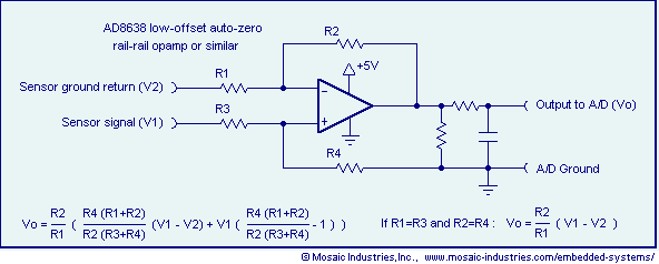
Ground loop offset errors and ground noise are eliminated by a differential amplifier or instrumentation amplifier before the analog-to-digital (A/D) conversion. The differential input amplifier addresses ground loop errors, allowing for precise measurement of non-isolated sensors. A simple operational...
It is a single integrated circuit that includes EEPROM, RAM, an analog-to-digital converter, numerous digital input and output lines, timers, and a UART for RS-232 communication, among other features. A complete programming environment is available for Linux, allowing programming...
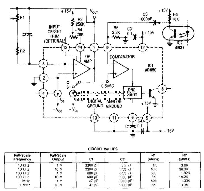
In this circuit, the input from the IC2 optocoupler is connected to the comparator input of the AD650 (Analog Devices or Maxim Electronics) voltage-to-frequency (V/F) converter. This converter internally generates a pulse that is sent to the operational amplifier,...
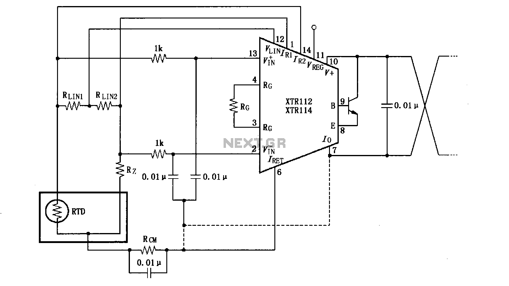
The length of the transmission wire in a current loop circuit can introduce radio frequency (RF) interference. This RF energy may lead to input errors in sensitive devices such as the XT112/114, causing instability in loop current or input...