
Integrated Circuit Voltage-to-Frequency Converter
The AD650 voltage-to-frequency and frequency-to-voltage converter is designed to provide high-performance conversion capabilities in various applications. Its architecture allows for a significant level of customization and adaptability, which is crucial for engineers working on precision measurement systems. The device's ability to maintain low linearity error across a wide frequency range makes it an excellent choice for high-resolution analog-to-digital conversion tasks.
The flexible input configuration supports multiple signal formats, which can be particularly beneficial in mixed-signal environments where different types of signals must be processed. The open-collector output design, along with a separate digital ground, enhances the device's compatibility with various logic families, making it easier to integrate into existing systems without significant redesign.
The AD650’s dynamic range of six decades is a noteworthy feature, allowing for the measurement of signals with vastly different amplitudes without sacrificing resolution. This capability is particularly useful in applications such as industrial automation, where signals may vary greatly.
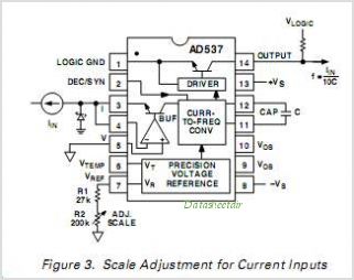
In applications requiring precise timing and frequency measurements, such as tachometers or FM demodulators, the AD650 excels due to its low offset voltage and user-programmable parameters. The ability to adjust input offset voltage to zero with an external potentiometer further enhances the accuracy of the device, making it suitable for demanding applications.
The availability of different packaging options, including DIP and PLCC, provides flexibility for designers regarding board space and thermal management. The device's specifications for various temperature ranges ensure its reliability in both commercial and industrial applications, thus broadening its usability across different sectors. Overall, the AD650 stands out as a versatile and robust solution for voltage-to-frequency and frequency-to-voltage conversion needs in modern electronic systems.The AD650 V/F/V (voltage-to-frequency or frequency-to-voltage converter) provides a combination of high frequency operation and low nonlinearity previously unavailable in monolithic form. The inherent monotonicity of the V/F transfer function makes the AD650 useful as a high-resolution Analog-to-digital converter.
A flexible input configuration al lows a wide variety of input voltage and current formats to be used, and an open-collector output with separate digital ground allows simple interfacing to either standard Logic families or opto-couplers. The linearity error of the AD650 is typically 20 ppm (0. 002% of full scale) and 50 ppm (0. 005%) maximum at 10 kHz full scale. This corresponds to approximately 14-bit linearity in an Analog-to-digital converter circuit. Higher full-scale frequencies or longer count intervals CAN be used for higher resolution conversions.
The AD650 has a useful dynamic range of six decades allowing extremely high resolution measurements. Even at 1 MHz full scale, linearity is guaranteed less than 1000 ppm (0. 1%) on the AD650KN KP, BD and SD grades. In addition to Analog-to-digital conversion, the AD650 CAN be used in isolated Analog signal transmission applications, phased locked-loop circuits, and precision stepper motor speed controllers. In the F/V mode, the AD650 CAN be used in precision tachometer and FM Demodulator circuits. The input signal range and full-scale output frequency are user-programmable with two external capacitors and one resistor.
Input offset voltage CAN be trimmed to zero with an external potentiometer. The AD650JN and AD650KN are offered in a plastic 14-pin DIP package. The AD650JP and AD650KP are available in a 20-pin plastic leaded chip Carrier (PLCC). Both plastic packaged versions of the AD650 are specified for the commercial (0C to +70C) temperature range. For industrial temperature range (-25C to +85C) applications, the AD650AD and AD650BD are offered in a ceramic package.
The AD650SD is specified for the full -55C to +125C extended temperature range. 🔗 External reference
Related Circuits

The circuit voltage source VREF excites the sensor bridge. The excitation voltage VEX is defined as VREF (1 + R1/R2), where the bridge is connected at both ends. The sensor bridge circuit is designed to convert a physical quantity, such...
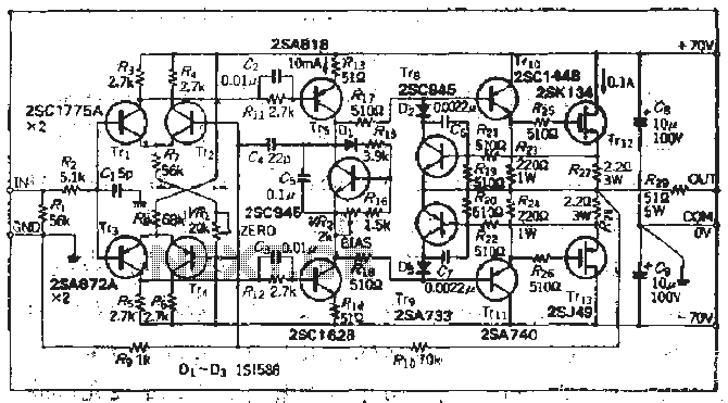
The south circuit consists of four parts, arranged in descending order: an NPN transistor dynamic garbage device (T1), a PNP transistor differential amplifier (T2, T3) forming a double differential circuit, two balanced output amplifiers with opposite phase, and a...
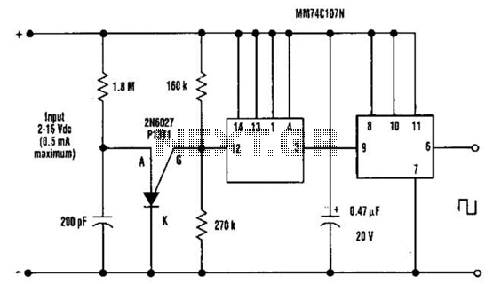
A direct current (DC) voltage source within the range of 2 to 15 volts can be converted into a unipolar square wave. This square wave has a peak amplitude that is nearly equal to the DC source voltage, with...
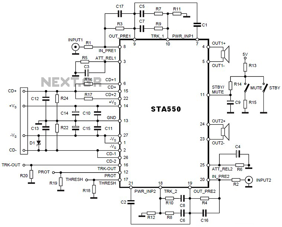
This is a 2 x 70W audio power amplifier circuit built using a single IC STA550. The amplifier circuit requires a few external components, primarily resistors and capacitors, and is straightforward to design. The STA550 audio amplifier can provide...
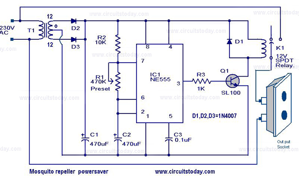
The circuit diagram of a mosquito repellent power saver circuit is provided along with a detailed explanation. The mosquito repellent power saver circuit is designed to efficiently operate a mosquito repellent device while minimizing energy consumption. This circuit typically integrates...
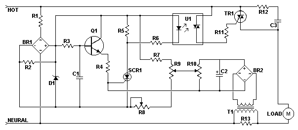
This AC motor speed controller can handle most universal type (brushed) AC motors and other loads up to about 250W. It works in much the same way as a light dimmer circuit; by chopping part of the AC waveform...
Warning: include(partials/cookie-banner.php): Failed to open stream: Permission denied in /var/www/html/nextgr/view-circuit.php on line 713
Warning: include(): Failed opening 'partials/cookie-banner.php' for inclusion (include_path='.:/usr/share/php') in /var/www/html/nextgr/view-circuit.php on line 713