
IRF9540N Gate Charge Test Circuit Schematic and Datasheet
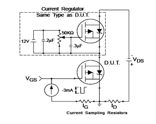
The IRF9540N Gate Charge Test Circuit is designed to evaluate the gate charge characteristics of the IRF9540N MOSFET. This circuit typically consists of a power supply, a resistor to limit the gate current, and measurement equipment to capture the gate charge waveforms. The gate charge, denoted as Qg, is critical for understanding the switching performance of the MOSFET, as it influences the turn-on and turn-off times.
The circuit operates by applying a voltage to the gate of the IRF9540N while monitoring the current through the gate resistor. The charge accumulated on the gate capacitance can be determined by integrating the gate current over time. The results provide insights into the efficiency of the MOSFET in various applications, particularly in high-frequency switching scenarios.
Furthermore, the datasheet's inclusion of the Switching Time Test Circuit and associated waveforms allows for a comprehensive analysis of the IRF9540N's performance in dynamic conditions. The Unclamped Inductive Test Circuit evaluates the device's response to inductive loads, while the Peak Diode Recovery dv/dt Test Circuit assesses the recovery characteristics of the body diode under high dv/dt conditions. Collectively, these tests provide a thorough understanding of the IRF9540N's operational limits and suitability for specific applications in power electronics.IRF9540N Gate Charge Test Circuitis schemed in the diagram below. IRF9540N is known to be rectifier device with advanced processing techniques to achieve extremely low on resistance per silicon area, according to the datasheet. Other thanGate Charge Test Circuit Schematic, you will find such Switching Time Test Circuit and Waveforms, Unclamped Ind
uctive Test Circuit, and Peak Diode Recovery dv/dt Test Circuit in the depth of the IRF9540 datasheet. 🔗 External reference
Related Circuits
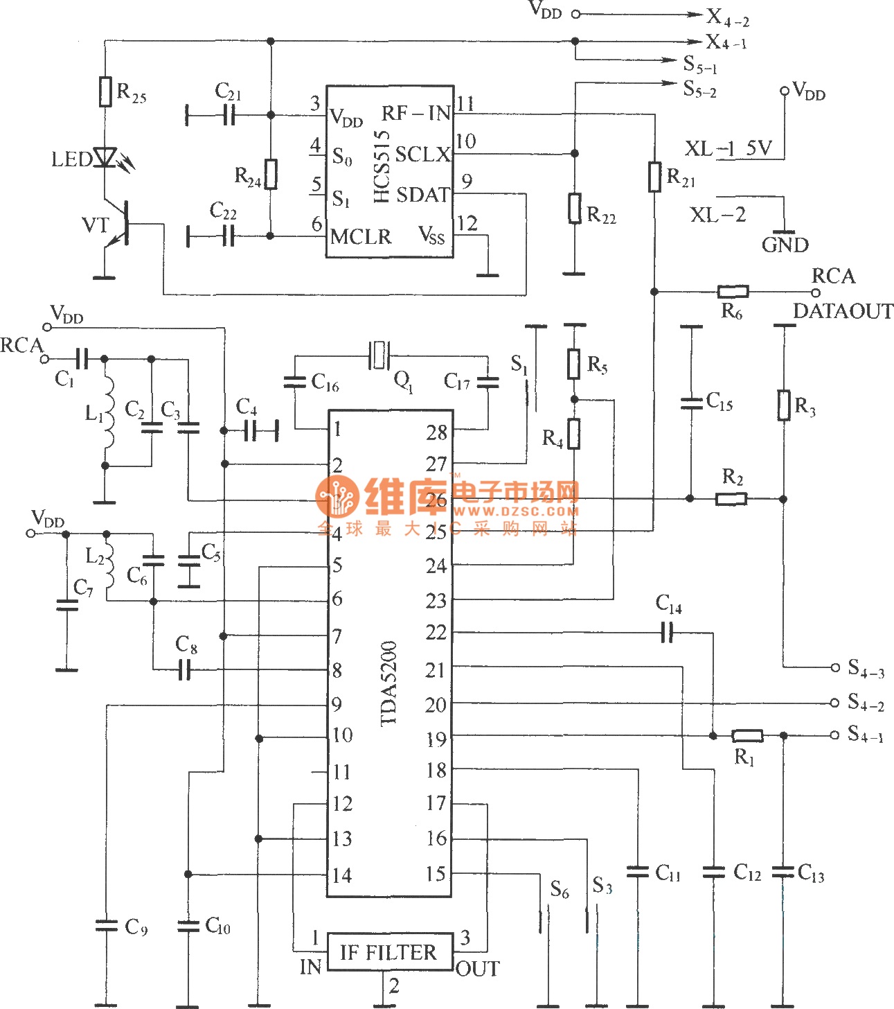
The TDA5200 is a low-power, single-chip ASK superheterodyne receiver circuit. It operates within two frequency blocks: 868 to 870 MHz and 433 to 435 MHz. This circuit is highly integrated, requiring minimal external components while offering excellent functionality. It...
Access to the resistors was available, and measurements indicated an open circuit when disconnected from any ground or input source. The circuit in question involves resistors that have been verified for accessibility. When measured in isolation—meaning they are not connected...
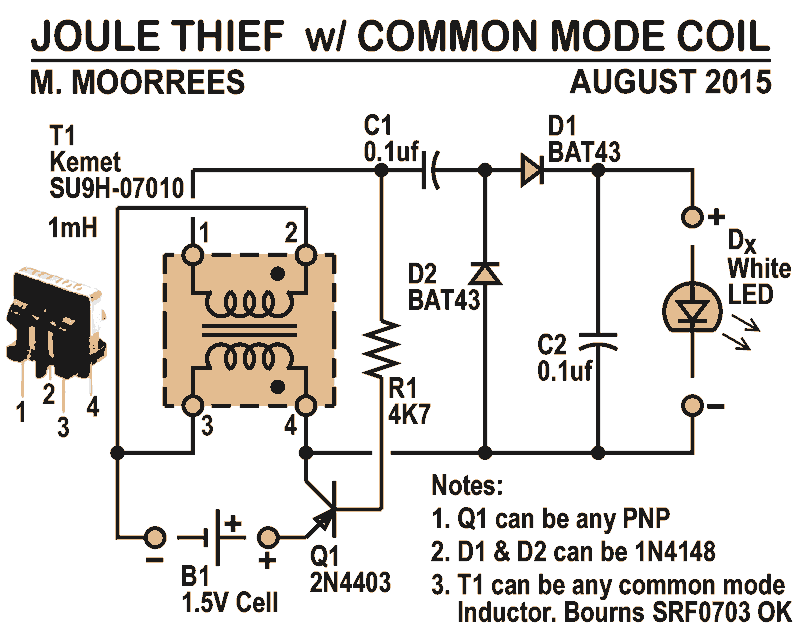
Like all joule thieves, this circuit boosts the voltage from a single 1.5V dry cell battery high enough to illuminate ultrabright GaN blue, green, or white LEDs. Instead of requiring a custom coil, it utilizes an off-the-shelf standard Kemet...
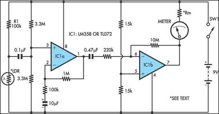
Strictly speaking, this simple circuit should not work. How could anyone expect an ordinary light-dependent resistor (LDR) photocell to detect the change in blood flow as the heart pulsates through a fingertip in natural daylight? The secret lies in...
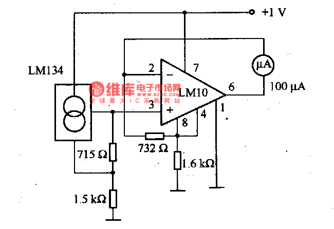
This is an electric thermometer circuit composed of the LM134. In the circuit, the voltage or current output by the LM134 is proportional to the thermodynamic temperature, which can be read on a 100 µA meter. The test temperature...
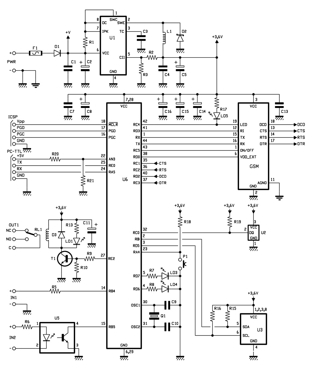
The complete GSM thermostat is controlled by a Microchip PIC18F46K20-I/PT microcontroller, which is programmed with firmware to manage temperature regulation and facilitate communication with the GSM module. This module, referred to as GSM, is a compact board that contains...