
Is it possible to use an NPN transistor to control a 5V power supply from Arduino

In this circuit configuration, the use of a PNP transistor or a P-channel FET is critical for efficient voltage regulation and switching. The PNP transistor operates by allowing current to flow from the emitter to the collector when the base is sufficiently forward-biased. The voltage drop across the emitter junction results in a lower emitter voltage compared to the base, which is a characteristic of bipolar junction transistors (BJTs). This voltage drop can affect the performance of the circuit, especially in precision applications.
On the other hand, the P-channel FET provides several advantages over the PNP transistor. Due to its field-effect operation, the P-channel FET exhibits higher input impedance, which minimizes the loading effect on preceding stages. When driven by a 5V logic level, the gate voltage controls the conductivity of the channel between the source and drain. The source is connected to the 5V supply, while the output is taken from the drain, allowing for efficient switching with minimal voltage drop. The low on-resistance of modern P-channel FETs further enhances efficiency, making them suitable for applications requiring high current capacity with minimal power loss.
In summary, the design choice between a PNP transistor and a P-channel FET depends on the specific requirements of the application, including voltage levels, current handling, and desired efficiency. The careful consideration of these factors will lead to optimal circuit performance and reliability.The emitter is always going to be a few hundred milli volts behind the base voltage (in this type of configuration) and as the base voltage is 5V, depending on how much current is taken by the "switched" circuit" on the emitter, it is more likely to be 4. 5V despite the collector being at 5V. However, if you used a PNP transistor with the emitter b eing fed by the 5V there is a fairly good chance that you can attain 5V (less maybe 10 or 20 millivolts) on the collector (load side) without much hassle. Better still use a P channel FET because this will do a slightly better job (maybe only a couple of millivolts "lost") and it can be fed directly from a 5V logic supply to its gate.
Source will connect to incoming 5V and output will be on drain. 🔗 External reference
Related Circuits
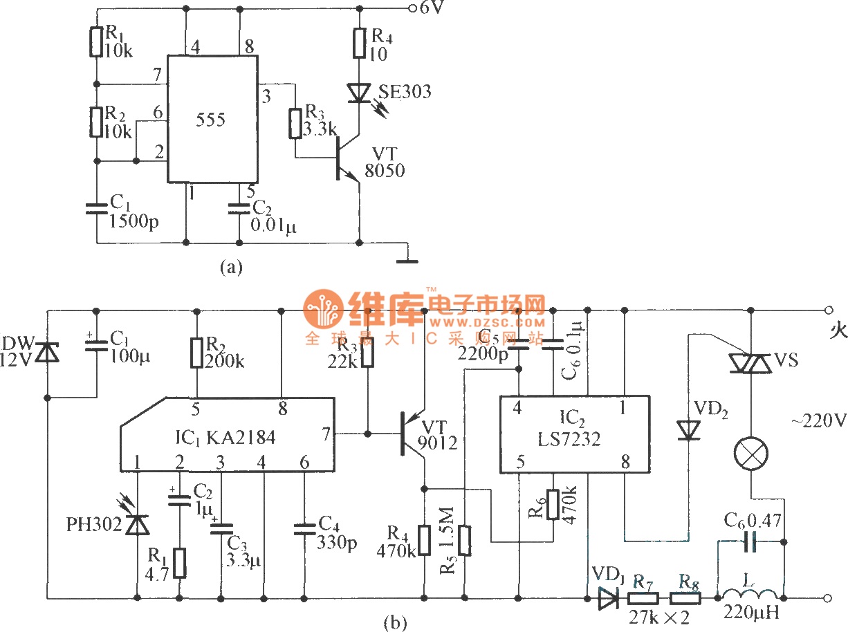
This is an infrared emission circuit diagram. The NE555 circuit generates a 40 kHz pulse, which is sent by the infrared emission control SE303 after being amplified by VT. The remote receiver and infrared dimming circuit are composed of...
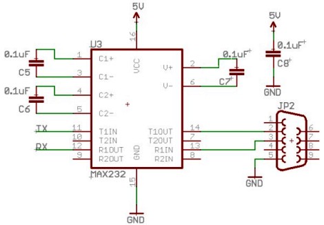
Select a free schematic drawing software that resembles the two mentioned. There have been discussions regarding circuit drawing software. Fritzing is favored, although it lacks certain components, such as the RS232 component. There is a request for feedback on...
When running large-scale software or games, a computer's internal temperature can increase significantly, especially during hot summer months. Although the machine is equipped with a CPU and graphics card fan, poor hot air circulation prevents immediate removal of heat...
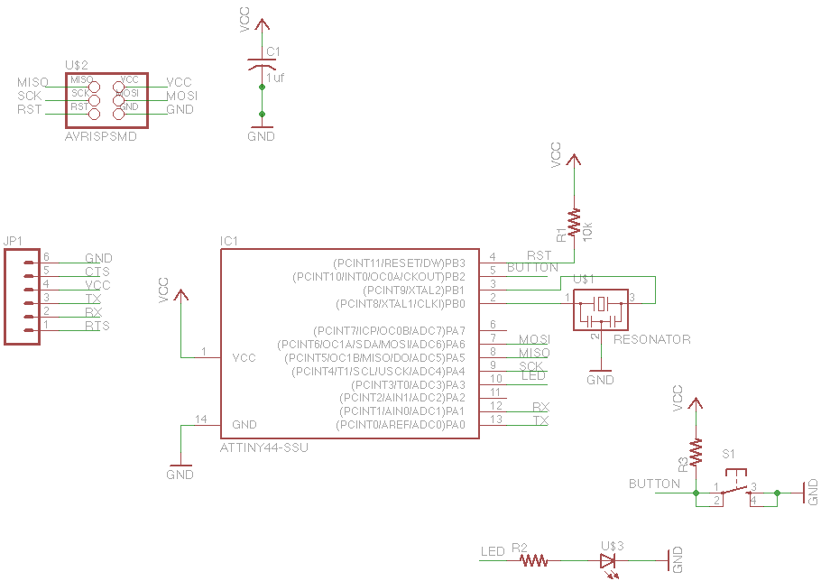
For this week's assignment, a chip design was provided, and the task was to incorporate a button and an LED (light-emitting diode). The objective was to fabricate the chip and program it to interact with the light and button....
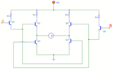
The transistors Q1, Q2, Q3, and Q4 form a bridge circuit. These are typically power transistors designed to handle high current. Transistors Q5 and Q6 drive the bridge. When input A is set high and input B is set...
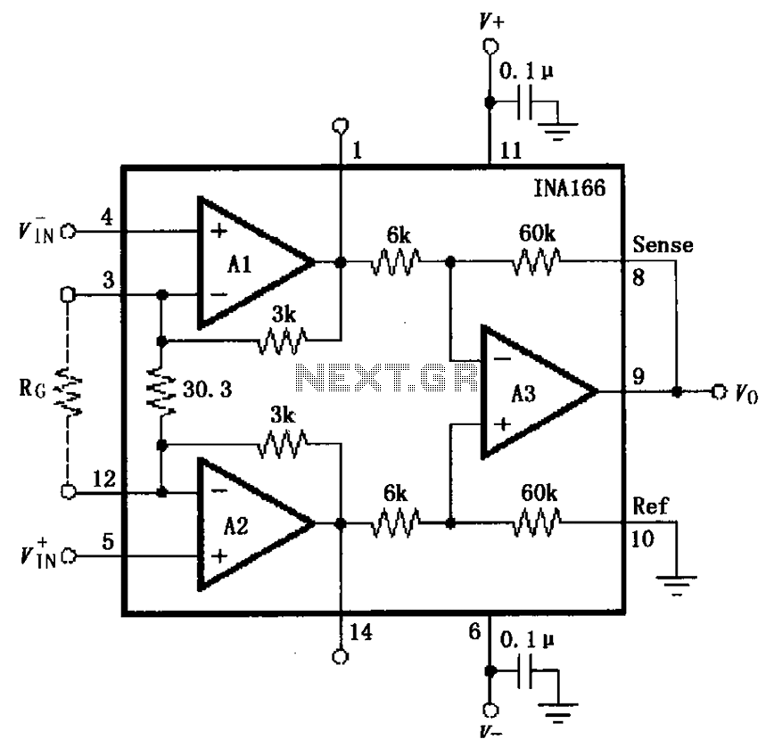
The basic connection circuit for the INA166 includes signal and power connections. A 0.1 µF tantalum capacitor should be used for filtering the chip's power supply terminal, and the PCB layout should be designed to position this capacitor as...