
Laser light detector

The laser light detector circuit is designed to provide high sensitivity and accurate detection of laser light. The phototransistor (Q5) serves as the primary sensor, detecting light intensity and converting it into an electrical signal. The configuration of the lens (LE2) ensures that the maximum amount of light is focused onto the phototransistor, enhancing the detector's responsiveness.
The sensitive amplifier stage, comprising the array (A1), is critical for amplifying the weak signals generated by the phototransistor. The biasing network formed by resistors R14 and R1 establishes the operating point of the amplifier, ensuring optimal performance. The Darlington pair configuration following Q5 serves to increase the input impedance and reduce loading effects on the phototransistor, allowing for better signal integrity.
The cascaded common-emitter amplifiers further increase the signal level, making it suitable for downstream processing. The sensitivity control resistor (R7) provides a means to fine-tune the detection threshold, allowing the user to adapt the circuit's response to different light sources or environmental conditions.
The integration of the output pulses via the one-shot circuit (Q1 and Q2) and capacitor C8 is a crucial step in converting the pulsed output from the amplifiers into a stable DC level. This DC signal is used to drive the relay drivers (Q3 and Q4), which control the relay (K1) that can switch external loads. The inclusion of the low-ohm resistor (R13) ensures that the relay can handle capacitive loads without arcing or damage during switching operations.
Finally, the ability to monitor the intercepted light beam through connector J2 enhances the functionality of the system, allowing for real-time audio feedback when working with pulsed light sources. This feature is particularly useful in applications involving precision alignment or monitoring of laser systems, ensuring that operators can make adjustments based on immediate feedback. Overall, the circuit is designed for robust performance in detecting and processing laser light signals, with features that enhance usability and reliability in various applications.The laser light detector utilizes a sensitive photo transistor (Q5) placed at the focal point of a lens (LE2). The output of Q5 is fed to a sensitive amplifier consisting of array (Al) and is biased via the voltage divider consisting of R14 and Rl.
The base is not used. Q5 is capacitively coupled to a Darlington pair for impedance transforming and is further fed to a capacitively coupled cascaded pair of common-emitter amplifiers for further signal amplification. Sensitivity control (R7) controls base drive to the final transistor of the array and hence controls overall system sensitivity.
Output of the amplifier array is capacitively coupled to a one-shot consisting of Ql and Q2 in turn integrating the output pulses of Q2 onto capacitor C8 through Dl. This dc level now drives relay drivers Q3 and Q4 activating K1 along with energizing indicator D3, consequently controlling the desired external circuitry.
The contacts of K1 are in series with low ohm resistor R13 to prevent Mure when switching capacitive loads. J2 allows "listening" to the intercepted light beam via headsets. This is especially useful when working with pulsed light sources such as GaAs lasers or any other varying periodic light source.
Related Circuits
This is an infrared (IR) proximity detector circuit. A matched infrared emitter and detector pair is used in this circuit. The voltage-controlled oscillator is involved. The infrared proximity detector circuit utilizes a matched pair of infrared emitter and detector components...
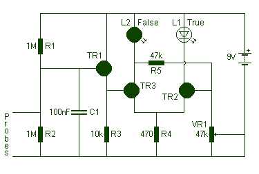
The circuit diagram of the Lie Detector is shown above. It consists of three transistors (TR1 to TR3), a capacitor (C1), two lights or LEDs (L1 & L2), five resistors (R1 to R5), and a variable resistor (VR1). This circuit...
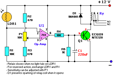
The provided schematic diagram illustrates an LM741 light/dark sensor circuit, derived from the 741 Op-Amp Tutorial by Tony van Roon. The ECG128/NTE128 transistor can be replaced with any NPN transistor that meets the necessary gain and current specifications for...
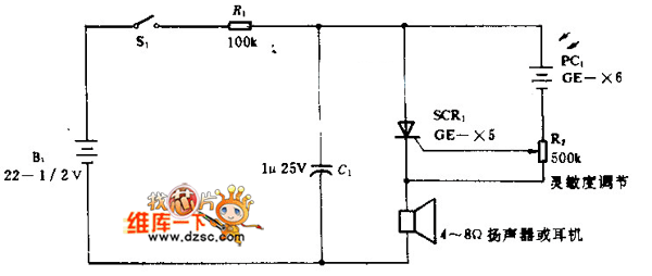
In the silicon-controlled trigger circuit, a cadmium sulfide cell is connected to a relaxation oscillator, which serves as a sensor to activate a blinking light in a darkroom. This setup causes a speaker to emit a warning sound of...
This circuit is designed to indicate, via a flashing LED, when room noise exceeds a predetermined threshold, which can be set to one of three fixed levels: 50, 70, or 85 dB. Two operational amplifiers (op-amps) are utilized to...

The Pulsed Multiple Gas (PMG) laser discussed in this chapter closely resembles the Home-Built Pulsed Argon and/or Krypton (Ar/Kr) Ion Laser from Scientific American. However, the PMG laser's developers have also utilized xenon (Xe) and oxygen (O2) and even...