
LC compliant boost converter circuit diagram
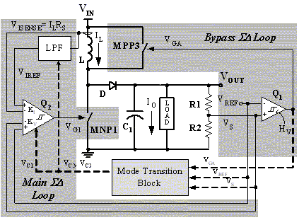
The described circuit employs a ΣΔ modulation technique for controlling the output voltage and inductor current in a power supply application. The main ΣΔ loop, managed by comparator Q2, effectively stabilizes the system by generating an internal variable s that is maintained at zero through feedback control. This feedback mechanism is crucial for ensuring that the output voltage remains stable under varying load conditions.
In steady state, the auxiliary switch MPP3 is kept open, preventing unnecessary switching losses and allowing the main loop to operate efficiently. The integration of the bypass ΣΔ loop, activated during transient events, enhances the system's response time by quickly adjusting the output voltage. Comparator Q1 plays a vital role in this process, detecting when the output voltage falls below a set threshold and adjusting the duty cycle of MPP3 to restore the voltage to the reference level VREF.
The operation of the bypass loop is particularly significant during load transients, where rapid changes in output voltage can occur. By forcing an increase in the average inductor current, the bypass mechanism compensates for these transients, ensuring that the output voltage remains within acceptable limits. The regulation of the inductor current by comparator Q2 ensures that the current remains at a constant value, preventing excessive power losses and output voltage ripple.
The overall design of this circuit exemplifies an effective approach to power management, balancing the need for fast transient response with the stability and efficiency of the main operating conditions. The careful regulation of inductor current and output voltage through the use of ΣΔ control techniques demonstrates a sophisticated understanding of power electronics principles.The main ΣΔloop, which again operates in steady state, is fully controlled by summing comparator Q2, which amplifies the ripples of the sensed inductor current and output voltage by gains KI and KV, respectively, to generate an internal variable s. This variable s , is regulated to zero by the feedback control action of Q2, as in conventional sliding-mode control.
In steady state, auxiliary switch MPP3 is always open and the bypass ΣΔ block containing comparator Q1 is inactive. The main loop gives wide LC filter compliance and low output voltage ripple since it adheres to the teachings of sliding-mode ΣΔ control. However, the transient response is slow because it is defined to meet the requirements of the worst-case LC specifications.
This slow response is corrected using the fast bypass ΣΔ loop during transient events. The bypass ΣΔ loop, operating during transient events only, is controlled by comparator Q1, which senses and controls the output voltage through the duty-cycle of switch MPP3. During bypass conditions, when the output voltage drops below the predefined window limit set by Q1, the bypass loop regulates the output voltage (VS) to VREF, irrespective of the inductor current, forcing the average inductor current to increase, since its dIL/dt is now mostly unidirectional.
This current consequently increases beyond its minimum average value ILMIN (inductor current IL equals ILMIN during steady-state conditions) and only drops back down when the output voltage again reaches its prescribed window limits, at which point MPP3 is disabled. Comparator Q2 only regulates the sensed inductor current to its reference value, which is the DC value of the sensed current.
This current loop is therefore independent and self-sustaining and the inductor current, as it is, is regulated and constant. A higher-than-minimum inductor current leads to increased power losses and a higher output voltage ripple, which is why the inductor current must be ultimately reduced to ILMIN.
🔗 External reference
Related Circuits
This inexpensive FM radio receiver antenna booster utilizes the BF324 TO92 style PNP transistor in a grounded-base configuration. The circuit can be employed as a... The FM radio receiver antenna booster circuit is designed to enhance the reception capabilities of...
This light-activated relay circuit utilizes the 555 timer integrated circuit (IC) and a light-dependent resistor (LDR) to create a light-sensitive relay suitable for applications such as intruder alarm systems or automatic lamp control at sunset and sunrise. The potentiometer...
The circuit is constructed on a breadboard and produces the expected sound characteristics, specifically a damped sine wave reminiscent of large 808/909-style kicks. However, it exhibits a significant amount of noise. An attempt was made to mitigate this by...
Assistance is needed in analyzing a circuit, specifically regarding the frequency cut-off between the bass and treble channels. The potential cut-off frequencies under consideration are 500Hz, 1KHz, or 5KHz. In audio processing circuits, the frequency cut-off point between bass and...

A simple touch dimmer circuit diagram using the TT6061 IC, which is a touch control integrated circuit used for light dimmer circuits and lamp dimmer circuits. The touch dimmer circuit utilizing the TT6061 IC is designed to provide a user-friendly...
This compact FM transmitter has a range of approximately 50 meters and is designed for hobbyists. With multiple mini-transmitters, users can create a diverse and engaging radio program. The device achieves high frequency stability due to its power supply...
Warning: include(partials/cookie-banner.php): Failed to open stream: Permission denied in /var/www/html/nextgr/view-circuit.php on line 713
Warning: include(): Failed opening 'partials/cookie-banner.php' for inclusion (include_path='.:/usr/share/php') in /var/www/html/nextgr/view-circuit.php on line 713