
LED flashing circuit for toys

The circuit utilizes a 4047 low-power monostable/astable multivibrator as the core timing component, configured in astable mode to generate a continuous square wave output. This output controls the flash rate of multiple LEDs, providing a visually dynamic display. The arrangement of the pins is crucial for the functionality of the circuit; pins connected to the power supply and ground establish the operating conditions, while the timing components, consisting of capacitors and resistors, define the frequency of oscillation.
The output from the 4047 is routed through resistors R6 and R7 to drive the bases of NPN transistors Q2 and Q3. These transistors act as switches for the Yellow LEDs, allowing them to turn on and off in sync with the timing pulses. The Q output from pin 10 and the Q-not output from pin 11 provide complementary signals, ensuring that the LEDs can be activated in a coordinated manner, enhancing the visual effect.
Transistor Q1 is utilized to control the Red LEDs, receiving its drive signal from pin 13 of the 4047 through resistor R8. The arrangement allows for a layered lighting effect, with the Yellow LEDs surrounding the Red LEDs, which are further complemented by Green LEDs connected to resistors R1 and R2. The design ensures that the current through each LED is limited by the respective resistors, preventing damage due to excessive current.
The power supply, PS1, is a 12VDC wall transformer that feeds the entire circuit, with a filter capacitor (C1) smoothing out any voltage fluctuations. The choice of components, including the wattage ratings of the resistors and the specifications of the capacitors, is critical to ensure reliable operation and longevity of the circuit. The construction of the printed circuit board (PCB) is a significant aspect of this project, requiring precision in layout and assembly to ensure proper functionality.
Attention to detail during assembly, including the placement of jumper wires and the careful handling of the CMOS IC to avoid static damage, is essential for the successful completion of the project. The final assembly not only requires soldering the components but also necessitates a thorough inspection before powering the circuit to confirm that all connections are correct and secure. It consists of a 4047 low-power monostable/astable multivibrator, IC1, used in the astable mode to provide the timing pulses to control the flash rate of the LEDs. To accomplish the astable mode, pins 4, 5, 6, and 14 are connected to +12VDC and pins 7, 8, 9, and 12 are connected to ground.
Pins 1 and 3 are connected to C2 and pins 2 and 3 are connected to potentiometer R9. A fixed value resistor can be used in place of the potentiometer R9, if the flash rate does not need to be adjusted. These three pins make up the R-C timing circuit. The output pulses from the 4047 are taken from pins 10, 11, and 13. Pin 10 is the Q output and pin 11 is the Q-not output. These two pins are onnected to R6 and R7 respectively. The collectors of Q2 and Q3 are connected to R4 and R5 respectively, which are connected to the cathodes of the Yellow LEDs. Pin 13 is the oscillator output and is connected to R8, which is connected to the base of Q1. The collector of Q1 is connected to R3, which is connected to the cathodes of the Red LED's. The emitters of the three transistors are connected to ground. The Green LEDs are connected to R1 and R2, which are connected to +12VDC. Resistors R1-R8 are current limiting resistors and the correct wattage for these resistors should be used to prevent excessive heat.
The resistive values may be changed to vary the brightness of the LEDs. The circuit is powered by PS1, a wall transformer, which is connected to a filter capacitor C1. It must be between 10 to 15 VDC and at least 500mA. Probably the most difficult part of this project is making the printed circuit board, Figure 2. The board used in the prototype took several hours to make using dry transfers. Using a different technique, such as photo resist, may be faster for the experienced hobbyist. Once the board is etched and drilled, the jumper wires should be placed on the board and soldered, as shown on Figure 3. Next the 84 Yellow LEDs should be placed around the border of the board, followed by the 42 Red LEDs that make up the heart and then the 16 Green LEDs that make up the letters I and U.
Resistors R1-R9 and capacitors C1and C2 should be placed on the board next and then the power supply, PS1. Sockets were used in the prototype for the I.C. and transistors. A socket for the I.C. is required, but the sockets for the transistors are not. Special care should be taken when handling the CMOS I.C., as a static discharge will destroy it. When you are finished soldering, check the board over for mistakes. If everything looks okay, apply power. Resistors R1, R2 - 470 ohm, 1/2-watt R3-R5 - 100 ohm, 3-watt R6-R8 - 1000 ohm, 1.4-watt R9 - 5000 ohm potentiometer Capacitors C1, C2 - 100uF, 16 volts, electrolytic radial Semiconductors IC1 - 4047, low power monostable/astable multivibrator Q1-Q3 - 2n3643 NPN transistor or equivalent Diodes LED1-LED84 - yellow light-emitting diode LED85-LED126 - red light-emitting diode LED127-LED142 - green light-emitting diode Other components PS1 - 12VDC @ 500mA wall transformer Miscellaneous: Jumper wire, solder, printed circuit board, drill and bits,14 pin I.C.
socket, and a frame or case. 🔗 External reference
Related Circuits

This is a simple circuit that illustrates the function of the programmable unijunction transistor. It can be quickly wired on a proto-board. The circuit utilizes a programmable unijunction transistor (PUT) to demonstrate its operation as an oscillator. The PUT, which...

This circuit is designed to drive an ultrasonic transducer. A question has arisen regarding how to limit the output current, as a 60W transducer may be at risk of damage due to excessive current. Guidance or examples for integrating...
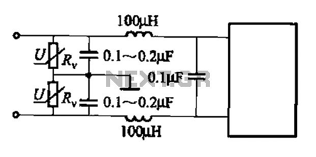
A common low-pass filter circuit is illustrated. Figures (a) to (c) demonstrate its ability to suppress high-frequency interference, while Figure (b) shows a varistor that can absorb lightning surge voltage. Figure (d) indicates the circuit's capability to suppress low...

A 2.5V voltage regulator circuit is illustrated, which is part of a computer's motherboard. The circuit employs an oscillation circuit with the RT9202 control core chip, converting a 5V input supply into a regulated +2.5V output voltage, with the...

Hello everyone, I am not well-versed in electronics, so I would appreciate it if someone could create a diagram for me. I would like to modify a circuit so that it can dial a number using speed dial and...
The ZN414 is an economical, single-chip AM radio integrated circuit introduced in 1972 by Ferranti. The TDA7000 is a monolithic integrated circuit designed for mono FM portable radios or receivers, focusing on minimizing size. Additionally, there is an FM...
Warning: include(partials/cookie-banner.php): Failed to open stream: Permission denied in /var/www/html/nextgr/view-circuit.php on line 713
Warning: include(): Failed opening 'partials/cookie-banner.php' for inclusion (include_path='.:/usr/share/php') in /var/www/html/nextgr/view-circuit.php on line 713