
led light flasher
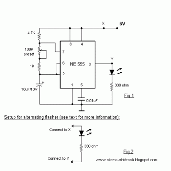
The circuit described revolves around an LED flashing mechanism controlled by a capacitor. The LED's flashing rate is determined by the RC time constant, which is influenced by the resistance (R) and capacitance (C) values in the circuit. In this scenario, the initial capacitor value of 10µF allows the LED to flash every half second. By increasing the capacitance to 22µF, the time constant increases, resulting in a longer flashing interval of one second.
To implement this circuit, a basic astable multivibrator can be utilized, which consists of an operational amplifier or a timer IC configured to oscillate. The LED is connected in series with a current-limiting resistor to ensure proper operation without exceeding its rated current. The resistor value should be calculated based on the supply voltage and the forward voltage drop of the LED.
The PCB design process involves several steps: First, the schematic diagram is created using the chosen PCB design software, ensuring all components are correctly connected. After verifying the design, the layout is generated, which includes the placement of traces, pads, and other necessary features. The design is then printed onto the chosen paper type.
When transferring the design to the PCB, it is crucial to ensure proper alignment and pressure during the heat application to achieve a successful transfer of the ink. After the transfer, the PCB must undergo an etching process to remove the unwanted copper, leaving only the desired traces for the circuit. This can be achieved using a suitable etching solution, such as ferric chloride, and requires careful handling and safety precautions.
Once the etching process is complete, the PCB can be cleaned and drilled for component placement. Components can then be soldered onto the PCB, completing the assembly of the flashing LED circuit. Proper testing should be conducted to ensure the circuit operates as intended, confirming the functionality of the LED flashing mechanism.With the preset at its max. the flashing rate of the LED is about 1/2 a second. It can be increased by increasing the value of the capacitor from 10uF to a higher value. For example if it is increased to 22uF the flashing rate becomes 1 second. Make a PCB in very easy steps. ! Create your PCB design using PCB designer software like Eagle, print out your design on photo paper or glossy paper with laserjet printer. Stick the printed design on the PCB (copper side) and then heat it using hot iron plate. The ink will stick on the PCB and it will be ready for etching process. Note: If you don`t have laserjet printer, then you can print the design on standard paper. Copy the printed design at Copy Service around your location (with glossy paper). 🔗 External reference
Related Circuits
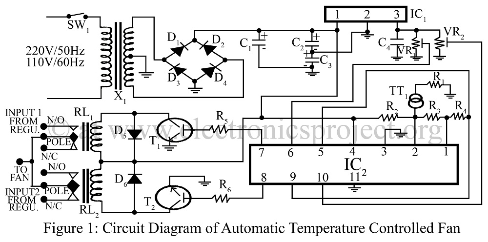
An automatic temperature-controlled fan regulates the fan speed based on temperature variations using the temperature transducer AD590 and an op-amp LM324 circuit diagram. The automatic temperature-controlled fan circuit utilizes the AD590 temperature transducer, which provides an output voltage that is...
This circuit will disconnect the line supply to audio or video equipment if there has been no input signal for approximately 2 seconds. Switch SI provides manual operation, while switch S2 functions as a reset mechanism. This circuit allows...
This circuit provides a simple visual indication of audio level signals, adaptable to various user requirements. It can be configured for different input levels, which can be adjusted using trimmer potentiometers TR1 (state) and TR2 (gain). The audio signals...
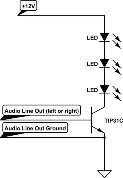
A circuit connects the line output (audio output) of a music-playing device to a large strip of approximately 200 LEDs, allowing them to flash in sync with the music. The circuit functions effectively when using a laptop as the...
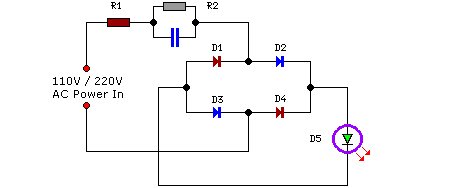
This is a straightforward and effective LED circuit that can be powered directly from an AC mains supply ranging from 100 volts to 230 volts. The circuit can serve as a mains power indicator or a night lamp. Resistors...
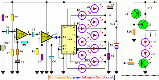
LED sequencer that follows the rhythm of music or speech, powered by a 9V battery, is a portable unit. The basic circuit illuminates up to ten LEDs in sequence, following the beat. The LED sequencer circuit operates by detecting audio...