
Leveraging FPGA and CPLD digital logic to implement analog to digital converters
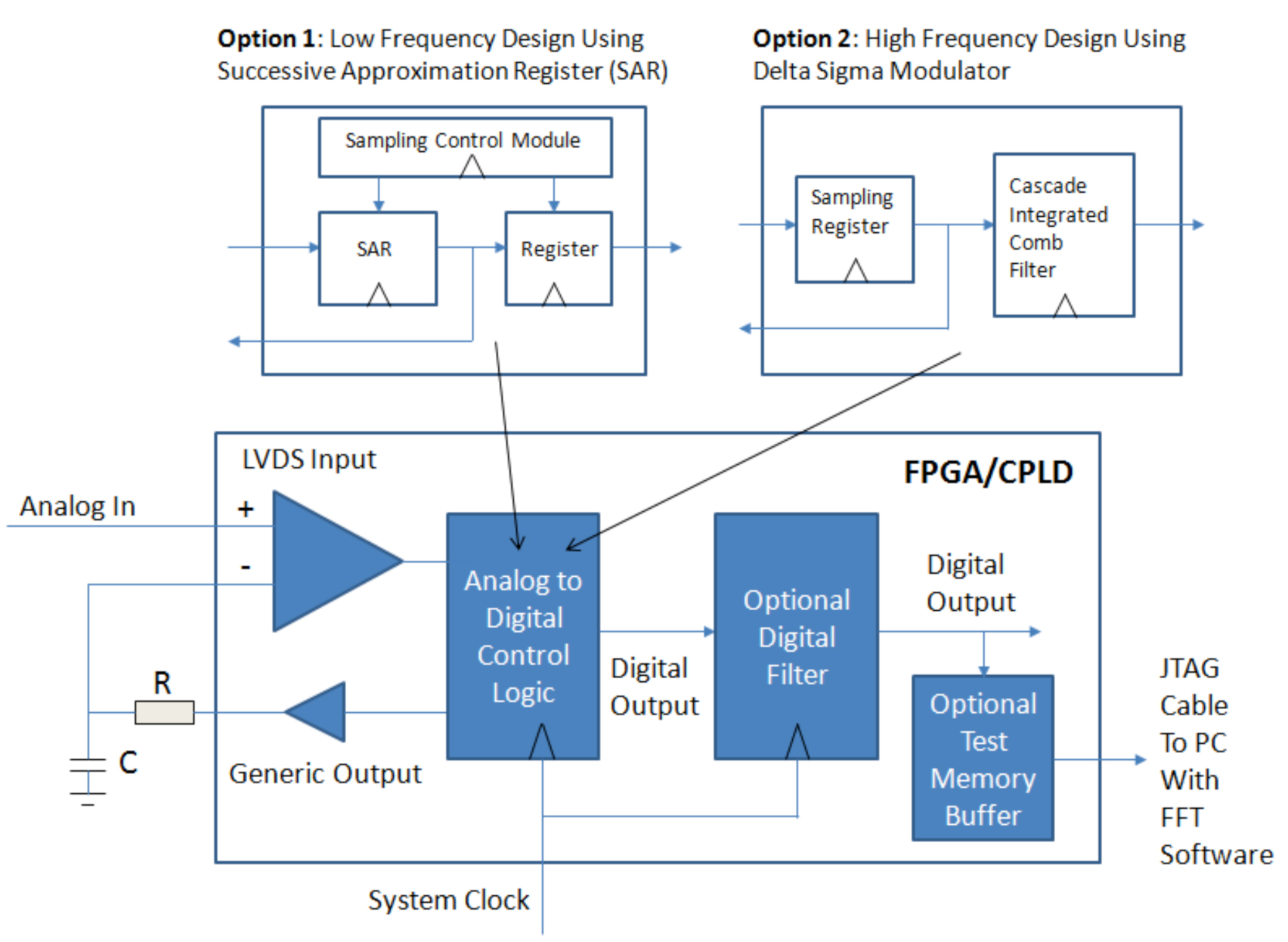
The implementation of an analog-to-digital converter (ADC) using FPGAs and CPLDs provides a versatile solution for interfacing digital systems with analog sensors. The process begins with the integration of an LVDS input, which serves as the interface for the analog signal. The RC circuit plays a critical role in shaping the input signal to determine the threshold for the comparator action. By adjusting the resistance and capacitance values, designers can tailor the response time and sensitivity of the ADC to meet specific application requirements.
For low-frequency applications, the successive approximation register (SAR) architecture is a common choice. This method allows for a precise and efficient conversion process, suitable for signals within the DC to 1 kHz range. The SAR ADC operates by iteratively comparing the analog input to a generated reference voltage, refining the digital output until the closest approximation of the input signal is achieved.
In contrast, higher frequency applications, such as those requiring sampling rates up to 50 kHz, benefit from the delta-sigma modulation technique. This approach leverages oversampling and noise shaping to achieve high resolution and accuracy. The combination of a sampling register and a CIC filter effectively reduces quantization noise, making it ideal for audio applications and other scenarios where signal fidelity is paramount.
Post-conversion, the digital output may be subjected to filtering processes to mitigate any residual high-frequency noise or artifacts that could compromise signal integrity. The optional memory buffer serves an important function in capturing the digital data for further analysis or debugging, allowing for real-time monitoring and adjustments during the development process.
The versatility of FPGAs and CPLDs in implementing ADC solutions underscores their significance in modern digital system design, offering robust capabilities to bridge the gap between digital logic and the analog world.Designers of digital systems are familiar with implementing the `leftovers` of their digital design by using FPGAs and CPLDs to glue together various processors, memories, and standard function components on their printed circuit board. In addition to these digital functions, FPGAs and CPLDs can also implement common analog functions using an LVDS
input, a simple resistor capacitor (RC) circuit and some FPGA or CPLD digital logic elements to create an analog to digital converter (ADC). The ADC is a common analog building block and almost always is needed when interfacing digital logic, like that in an FPGA or CPLD, to the `real world` of analog sensors.
This article will explain the implementation of both a low frequency (DC to 1K Hz) and higher frequency (up to 50K Hz) ADC using reference designs and demo boards available from Lattice Semiconductor. A sample application for each design: one for a system monitor in a network switch, and another for frequency detection in an audio communication system, will be examined.
A simple analog to digital converter can be constructed by adding a small RC circuit to an LVDS input on an FPGA or CPLD. As illustrated in the bottom left of figure 1, the RC network is placed on one side of the LVDS input and the Analog Input of interest is placed on the other side.
The LVDS input will act as a simple analog comparator and will output a digital `1` if the analog input voltage is higher than the voltage from the RC network. By changing the voltage on the input to the RC circuit (from the generic output of the FPGA/CPLD), the LVDS comparator can be used to analyze the analog input voltage to create an accurate digital representation.
The analog to digital control module can be implemented in a variety of ways, depending on the frequency of the Analog Input, the desired resolution and the logic resources available. A low frequency signal can be processed using a simple successive approximation register, as shown in option 1 at the top left of figure 1.
A higher frequency implementation, shown on the top right of figure 1, can be implemented using a delta sigma modulator function, which consists of a sampling register and a cascade integrated comb (CIC) filter. Once the digital signal has been constructed, the digital output can be optionally filtered to remove any unwanted high frequency components introduced by system noise or feedback jitter (explained in more detail below).
After the optional digital filter block, an optional memory buffer can be used for debug/testing purposes. The digital output can be sampled by the memory buffer and then scanned out via a JTAG port into a personal computer running signal analysis software.
🔗 External reference
Related Circuits
Both converters utilize CMOS inverters. Figure 105-1A illustrates a free-running circuit where both pulse duration and pulse pause are influenced by the temperature of diode D8. This configuration is suitable for applications where synchronization between the converter and other...
The Single-Ended Primary Inductance Converter (SEPIC) topology is an effective solution for automotive power systems that necessitate an output voltage that falls between the low and high values of the input voltage. The SEPIC topology is suitable for this...
This Project Digital Calendar using Microcontroller is an advanced digital calendar, which displays the Date, Day, Month over the LED display. It has an 8 bit Microcontroller which runs on the Program embedded on its ROM. Separate LEDs are...
This circuit is a stable frequency counter with an accuracy of 5 significant digits. It operates within a frequency range of 0 to 30 MHz and has an input sensitivity greater than 100 mV. The probe connects to the...
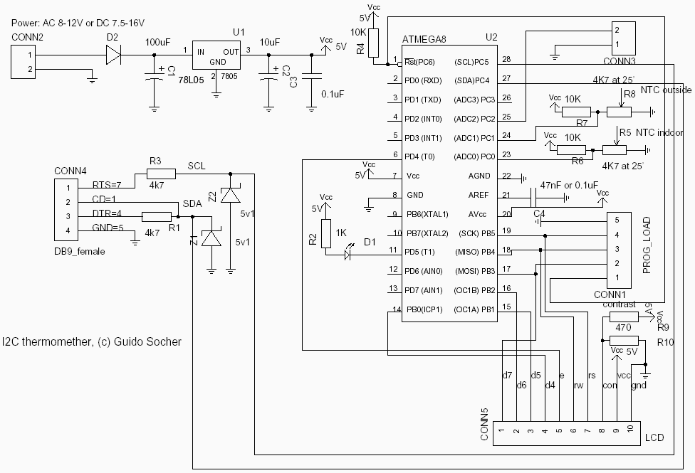
The Atmega8 microcontroller from Atmel features numerous digital and analog input/output lines, making it an ideal choice for developing various measurement equipment. It is essential to have the GCC AVR programming environment installed, as outlined in the article "Programming...
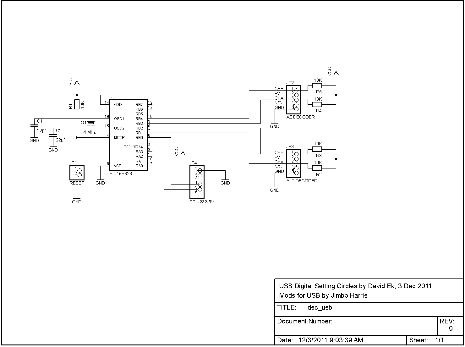
The serial version of the DSC circuit described in these pages is easily adaptable for use with a USB-serial conversion cable. FTDI manufactures the TTL-232R-5V cable, which converts TTL-level serial data directly from the PIC to USB for connection...
Warning: include(partials/cookie-banner.php): Failed to open stream: Permission denied in /var/www/html/nextgr/view-circuit.php on line 713
Warning: include(): Failed opening 'partials/cookie-banner.php' for inclusion (include_path='.:/usr/share/php') in /var/www/html/nextgr/view-circuit.php on line 713