
Light dimmer circuit
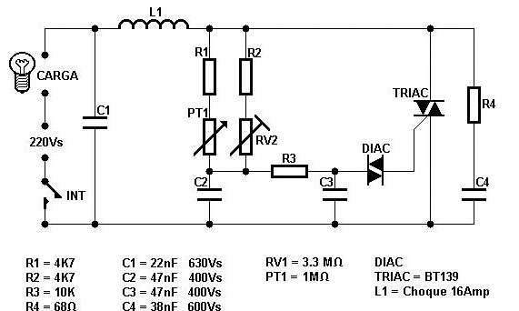
This circuit schematic represents a solid-state light dimmer designed to modulate the brightness of incandescent lamps through phase control. The circuit operates on a 220V AC mains supply, which necessitates careful handling due to the potential hazards associated with high voltage. The primary component responsible for controlling the light output is the triac, which is triggered by a DIAC that conducts after its breakdown voltage is reached.
The circuit's operational principle hinges on the adjustment of the duty cycle, which is achieved by manipulating the variable resistances R1, PT1, R2, and RV2. This configuration allows for precise control over the timing of the triac's activation, thereby influencing the effective power delivered to the light bulb. Capacitors C1 and C2 play a critical role in establishing the timing delay necessary for the DIAC to fire, while also contributing to the overall stability of the circuit.
The inclusion of an RF interference filter, consisting of capacitor C1 and inductor L1, is essential for minimizing electromagnetic interference generated during the triac's operation. Additionally, the RC snubber network formed by R4 and C4 serves to protect the triac from unintended triggering due to voltage spikes, enhancing the reliability of the circuit.
To ensure optimal performance and safety, it is crucial that the circuit is calibrated correctly. The initial setup involves adjusting PT1 to its maximum resistance while setting RV2 to achieve the desired minimum brightness. This calibration step is vital for establishing a functional range for the dimmer, allowing for smooth transitions between different brightness levels.
The triac BT139, chosen for this application, provides robust performance under continuous operation, provided it is adequately heat-sinked. Careful attention to component ratings and thermal management is essential for maintaining circuit integrity and ensuring safe operation. This circuit design exemplifies the principles of phase control dimming, providing an efficient solution for adjustable lighting applications.This circuit design is not tested by staff. The circuit design as submitted by the designer is believed to be correct, but there is no guarantee of the correctness of the circuit design. The contents of the articles below might be totally inaccurate, inappropriate, or misguided. There is no guarantee as to the suitability of said circuits and information for any purpose. Warning: This circuit operates at potentially lethal 220V AC mains voltage. The circuit should be built and used only by people who know hot to safely work with such dangerous voltages and how to built the circuit so that it is safe to use. Solid-state light dimmers work by varying the "duty cycle" (on/off time) of the full AC voltage that is applied to the lights being controlled.
For example, if the voltage is applied for only half of each AC cycle, the light bulb will appear to be much less bright than when it get the full AC voltage, because it get`s less power to heat the filament. Solid-state dimmers use the brightness knob setting to determine at what point in each voltage cycle to switch the light on and off.
The exact time when the triac is triggered relative to the zero crossings of the AC power is used to determine the power level to the light bulb. When the the triac is triggered it keeps conducting until the current passing though it goes to zero (exactly at the next zero crossing if the load is purely resistive, like light bulb).
By changing the phase at which you trigger the triac you change the duty cycle and therefore the brightness of the light. The circuit contains a variable resistance that consists of R1 + PT1 in paralle with R2 + RV2. This variable resistance together with capacitors C1 and C2 form a delay from the mains zero crossing to the firing point of the diac.
DIAC is a bidirectional trigger diode that conducts current only after its breakdown voltage (typically around 30V) has been exceeded momentarily. The larger the variable resistance feeding the capacitors, the longer it takes for the voltage across the capacitor to rise to the point where the DIAC fires turning on the triac TH1.
The circuit is calibated in such way that first PT1 is turned to highest resistance values. The value of RV2 is turned in such position that the desired minumum brightness of the light bulb is reached. After this calibration the PT1 can be used to freely control the light bulb brightness at the desired control range form the maximum brightness to set minumum.
Capacitor C1 and inductor L1 make a simple radio frequency interference filter. Without it the circuit would generate quite much interference because firing of the triac in the middle of the AC phase causes fast rising current surges. The triac BT139 used in the circuit is rated for 16A continuous current when properly cooled with a large heat sink.
The maximum current is less with less cooling. The components R4 and C4 for a RC nubber network that protects TRIAC from spurious triggering. 🔗 External reference
Related Circuits

This is a simple design of an audio level meter. The circuit utilizes a single integrated circuit (IC) and a minimal number of external components. It is based on the LM3915, which functions as the controller for the audio...
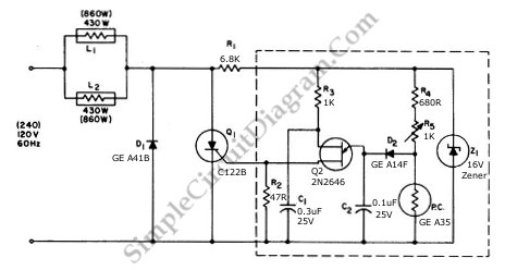
This circuit utilizes a controlled half-plus-fixed half-wave phase control method to regulate an 860-watt lamp load, allowing operation from half to full power. The circuit employs a phase control technique, which involves adjusting the phase angle of the AC...

A 27MHz transmitter circuit schematic utilizing the MC2833 and two FET transistors, MPF6660. This design incorporates a Motorola MC2833 one-chip FM transmitter along with several supporting components. The 27MHz transmitter circuit is designed to operate within the FM radio frequency...
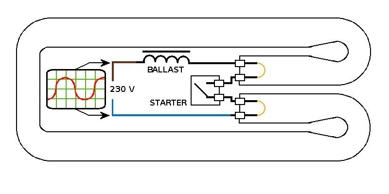
The magnetic field generated in the ballast collapses rapidly, resulting in a high voltage across the tube, which causes the internal gas to conduct. This process can be likened to gradually inflating a balloon and then puncturing it with...
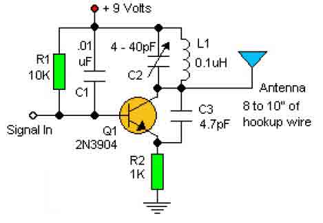
This basic RF oscillator circuit is easy to build and the components are not critical. Most of them can be found in your junk parts box. The L1 antenna coil can be made by close winding 8 to 10...
The circuit consists of a NE555 timer and a frequency modulation circuit that modifies the self-excited multivibrator NE555 by adjusting the charging current for frequency modulation. The components VT1 and VT2 form a current mirror circuit, which generates a...