
Long-Duration Time Delay

The circuit described utilizes a combination of a bipolar junction transistor (BJT) and a field-effect transistor (FET) to create a highly adjustable timing mechanism. The primary component, transistor Q1, works in conjunction with resistors R1, R2, and R3 to establish a constant current source. This current source is capable of being fine-tuned to deliver a minimal charge current, which is particularly beneficial for applications requiring low power consumption.
The adjustment capability allows the circuit to operate at very low current levels, which is crucial for applications where energy efficiency is paramount. However, the current level must remain below the threshold necessary to trigger the UJT, which requires a peak current of 0.2 A. To circumvent this limitation, an external source can be employed to provide the necessary peak current when required.
Field-effect transistor Q2 serves a critical role as a source follower, ensuring that the current flows smoothly into the emitter lead of the UJT prior to its activation. This configuration aids in maintaining the integrity of the timing sequence by controlling the discharge of capacitor Ce through diode D1. The selection of diode D1 is essential; it must exhibit a leakage current that is significantly lower than the charge current to ensure that the timing mechanism operates effectively without premature triggering.
The circuit's design also incorporates a variable resistor R1, which dictates the voltage across R3 and the base-emitter junction of Q1. This voltage setting is vital for establishing the timing characteristics of the circuit. The delay time, which can extend up to 10 hours, is directly influenced by the resistance value of R3. As IB remains small, the relationship between delay time and R3 is linear, providing predictable and controllable timing intervals.
Finally, resistor R4 is integrated into the circuit as a safeguard. It is placed in series with the drain terminal of the FET and is required to have a sufficiently high resistance to limit the current flow when the UJT is activated. This precaution prevents the UJT from remaining in an 'on' state, which could lead to circuit latching and malfunction. Overall, this circuit design effectively combines various components to create a reliable and adjustable timing mechanism suitable for low-power applications. Transistor Ql and resistors Rl, R2, and R3 form a constant current source and the charge current might be adjusted to be as low as a few nanoamperes. This current would, of course, not be sufficient to fire the UJT where IP=0.2 A, unless the peak current was supplied from another source. Field-effect transistor Q2, acting as a source follower, supplies the current flowing into the emitter lead prior to firing and diode Dl provides a low-impedance discharge path for Ce- Dl must be selected to have a leakage that is much lower than the charge current.
Because IB is small, the delay time will vary linearly with R3. The voltage (E), applied across R3 and the base-emitter junction of Ql, is set by the variable resistor Rl. Time delays up to 10 hours are possible with this circuit. Resistor R4, in series with the FET drain terminal, must be large enough not to allow currents in excess of Iy to flow when the UJT is on.
Otherwise, the UJT will not turn off and the circuit will latch up.
Related Circuits

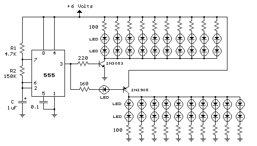
This circuit features an adjustable output timer capable of re-triggering at specified intervals. The output duration can range from a fraction of a second to over half an hour, and it can be configured to repeat at regular intervals...
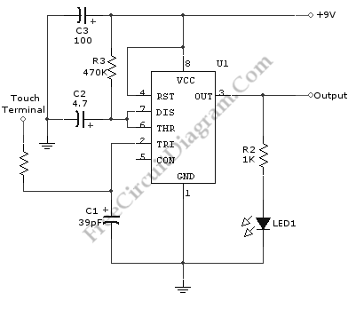
A schematic diagram of a touch switch circuit is presented. This circuit comprises a timer, a one-shot multivibrator, and a touch terminal. The timer utilized in this circuit is a 555 timer, which is connected to the one-shot multivibrator....
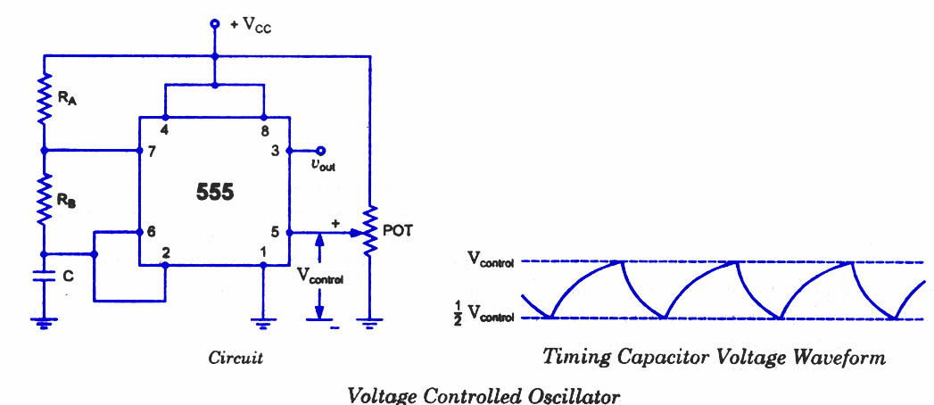
As discussed in previous blog posts, the pin 5 terminal serves as a voltage control terminal, allowing for the adjustment of threshold and trigger levels. Typically, the control voltage is set at +2/3VCC due to the internal voltage divider....
The SE555/NE555 timer was first introduced by Signetics Corporation around 1971. The pin connections and their functions are as follows: Pin 1 (Ground) is the most-negative supply potential and is typically connected to circuit common when powered by positive...
The cumulative timer circuit comprises resistor R1 and an internal crystal oscillator, represented in a chart. Resistors R1 and R2 are metal film types, while resistors R3 to R5 are rated at 1/8W and also of the metal film...

The purpose of this prototype unit is to eliminate the need for an oscillator. It provides a mains-derived and fully variable 50 Hz AC voltage, adjustable down to millivolts for comparison and accuracy testing of two or more parallel-connected...