
long range fm transmitter circuit
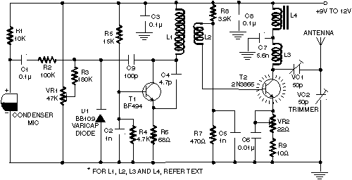
The circuit design begins with the oscillator stage, utilizing transistor T1 (BF494), which is configured in a common-emitter arrangement to achieve variable frequency operation within the VHF range. The inclusion of a varicap diode allows for fine-tuning of the frequency, enabling the transmitter to modulate audio signals effectively. The output from the oscillator is fed into the base of transistor T2 (2N3866), which is configured as a class A amplifier. This transistor is responsible for increasing the power of the signal, with the gain typically ranging from four to five times, resulting in the desired output power.
To ensure optimal signal transmission, the circuit should be assembled on a high-quality substrate, such as glass epoxy, which minimizes signal loss and enhances durability. The use of an aluminum enclosure not only protects the circuit from external interference but also aids in thermal management. The aluminum sheet shielding around the oscillator stage is crucial for preventing unwanted oscillations and ensuring stable operation.
The circuit design incorporates two potentiometers: VR1 for frequency adjustment and VR2 for power control. Proper adjustment of these components is essential for achieving the desired operational parameters. The trimmers VC1 and VC2 allow for fine-tuning of the oscillator frequency and output power, respectively, ensuring that the transmitter operates efficiently.
Power supply considerations are critical; a 12V rechargeable battery pack consisting of 10 x 1.2-volt Ni-Cd cells provides a reliable and stable voltage source. This arrangement not only supports the operational requirements of the circuit but also enhances portability. The heat sink for transistor T2 is necessary to dissipate heat generated during operation, preventing thermal runaway and ensuring longevity.
In summary, this transmitter circuit is designed for effective VHF signal transmission with adjustable frequency and power output. Proper assembly, tuning, and thermal management are essential for achieving optimal performance and reliability in communication applications.The transmitter ambit declared actuality has an added RF ability amplifier stage, afterwards the oscillator stage, to accession the ability achievement to 200-250 milliwatts. With a acceptable analogous 50-ohm arena even antenna or multi-element Yagi antenna, this transmitter can accommodate analytic acceptable arresting backbone up to a ambit of
about 2 kilometres. The ambit congenital about transistor T1 (BF494) is a basal low-power variable-frequency VHF oscillator. A varicap diode ambit is included to change the abundance of the transmitter and to accommodate abundance accentuation by audio signals.
The achievement of the oscillator is about 50 milliwatts. Transistor T2 (2N3866) forms a VHF-class A ability amplifier. It boosts the oscillator signals ½ ability four to bristles times. Thus, 200-250 milliwatts of ability is generated at the beneficiary of transistor T2. For bigger results, accumulate the ambit on a good-quality bottle adhesive lath and abode the transmitter central an aluminium case. Shield the oscillator date application an aluminium sheet. Potentiometer VR1 is acclimated to alter the axiological abundance admitting potentiometer VR2 is acclimated as ability control.
For hum-free operation, accomplish the transmitter on a 12V rechargeable array backpack of 10 x 1. 2-volt Ni-Cd cells. Transistor T2 charge be army on a calefaction sink. Do not about-face on the transmitter after a analogous antenna. Adjust both trimmers (VC1 and VC2) for best manual power. Adjust potentiometer VR1 to set the axiological abundance abreast 100 MHz. 🔗 External reference
Related Circuits
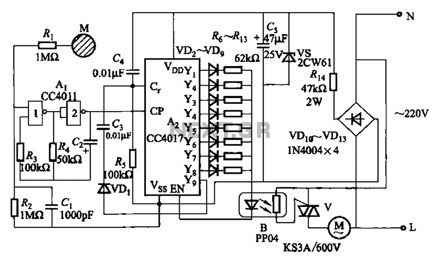
The circuit depicted in Figure 3-7 utilizes a touch sensor chip in conjunction with a conductive sheet. It is designed to achieve eight different speed settings. The CC4011 timing pulse oscillator is comprised of an integrated circuit. The configuration...
In this lab, flip-flops will be utilized. Xilinx provides a comprehensive library of sequential circuits, which is recommended for circuit searches: Xilinx Reference Library. The objective of this lab is to implement a sequential circuit that controls three LEDs:...
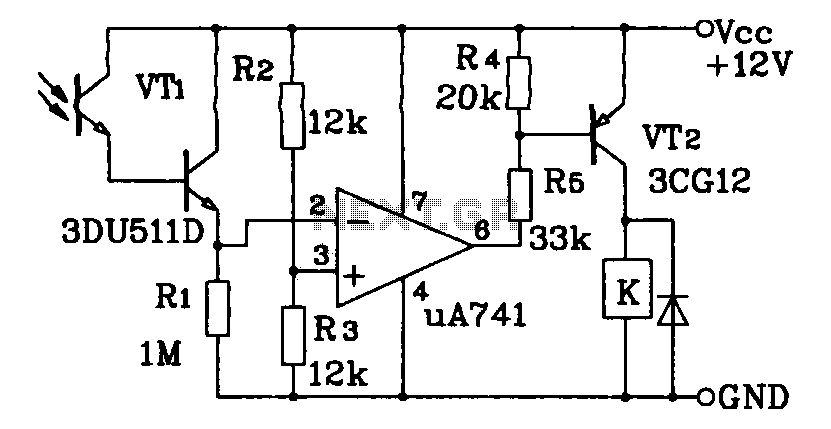
This circuit application utilizes a Darlington phototransistor for light-triggered switching. The design incorporates a Darlington phototransistor and an operational amplifier (op-amp), allowing the circuit to respond to very faint light levels. The circuit can be modified to trigger in...

By adjusting the oscillators so their frequencies are very nearly the same, the difference between them is made audible as a beat note. This beat note changes slightly when the search loop is moved over or near to a...
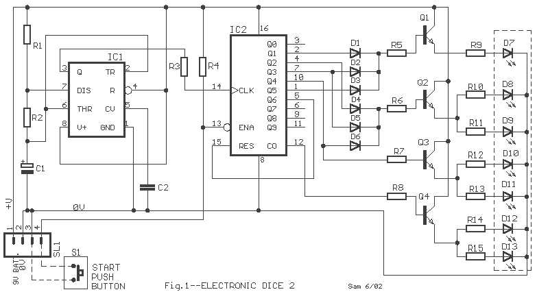
The IC1 is a 555 timer IC connected for astable operation. The clock pulses are fed to the IC2 via the 10K resistor. The IC2 is a 10-stage counter; output 6 (pin 5) is connected to RESET (pin 15),...
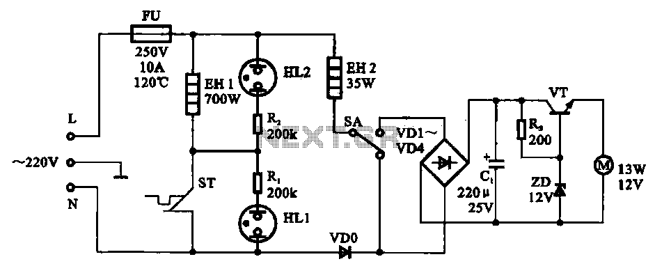
The electric thermos temperature detection control circuit is designed to monitor and manage the temperature within an electric thermos. It primarily consists of a control circuit for the boiler heater and heater insulation, an electrical magnetic pump motor drive...