
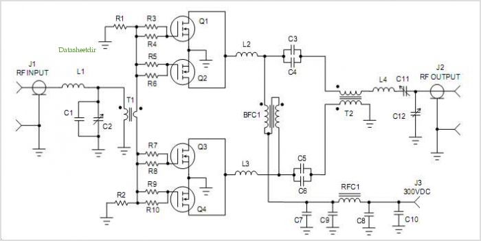
Low Cost 1000 Watt 300 Volt Rf Power Amplifier For 27.12mhz
The LNK306PN is a highly integrated power supply solution designed for efficient LED driving applications. It features a constant current output, making it ideal for driving LED arrays where consistent brightness is crucial. The maximum output voltage of 70 VDC allows for versatility in various LED configurations. The passive valley-fill PFC circuit incorporated into the design not only improves the overall efficiency of the power supply but also minimizes harmonic distortion, thus enhancing compatibility with sensitive electronic devices.
The implementation of EN55015B EMI standards within the design ensures that the power supply operates without generating excessive electromagnetic interference, which could disrupt other electronic equipment. The use of a line fuse (F1) provides an essential safety feature, protecting the circuit from overcurrent conditions that could lead to damage or failure.
Differential filtering capacitors (C6 and C10) play a critical role in smoothing the output voltage and reducing noise, thereby enhancing the stability of the LED drive current. The inclusion of inductors (L1 and L2) and resistors (R15 and R16) further mitigates EMI, ensuring that the power supply meets stringent regulatory requirements.
Full-wave rectification, achieved through diodes (D5-D8), converts the AC input into a stable DC output, which is crucial for LED operation. The valley-fill circuit, comprising diodes (D2, D3, and D4) and capacitors (C1 and C2), enhances the power factor by allowing the circuit to draw current more efficiently, thus reducing energy losses.
The ON/OFF control mechanism utilized by the LNK306PN optimizes performance by regulating the output current. When the feedback pin (FB) detects a current exceeding 49 A, it disables the MOSFET, preventing potential damage to the circuit. This feedback mechanism ensures that the power supply operates within safe limits, providing reliable performance over time.
Overall, the LNK306PN power supply is an advanced solution for LED driving applications, combining efficiency, safety, and compliance with industry standards to deliver exceptional performance.The LinkSwitch-TN supply LNK306PN shown in Figure 1 provides a constant current output of up to 9 W at a maximum output voltage of 70 VDC, ideal for driving LEDs A passive valley- ll power factor correction (PFC) circuit gives the supply a power factor greater than 0. 92, which meets requirements of ENERGY STAR SSL for commercial applications. C are has been taken such that the supply also meets EN55015B EMI requirements. Line fuse F1 protects the power supply in case of catastrophic failures. Capacitors C6 and C10 provide differential ltering. EMI is mitigated by inductors L1 and L2 along with resistors R15 and R16. Full wave recti cation is accomplished by Diodes D5-D8. Diodes D2, D3 and D4, along with capacitors C1 and C2, form the valley ll circuit and provide power factor correction. The LNK306PN device uses an ON/OFF control method. Whenever current in excess of 49 A is delivered into the FB pin of U1, MOSFET switching is disabled. Upon the device`s next internal Clock cycle, the FB pin current is sampled, and if it is below the 🔗 External reference
Related Circuits
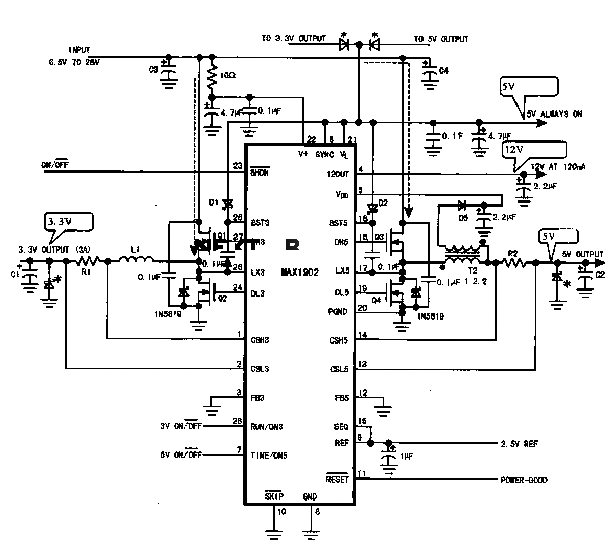
Multi-output power supply circuit (MAX1902). This circuit illustrates the power supply configuration for a notebook computer motherboard, utilizing the MAX1902 chip for power control. It is designed to convert the battery's DC voltage into multiple DC voltage outputs. The multi-output...
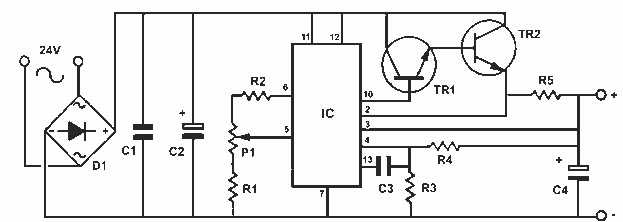
This is a very useful project for anyone working in electronics. It is a versatile power supply that will solve most of the supply problems arising in the everyday work of any electronics workshop. It covers a wide range...
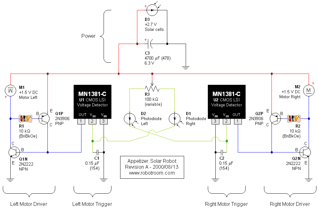
A light-seeking solar-powered tiny robot based on a BEAM design. The article includes pictures, links, a video, and a schematic. The described robot employs a BEAM (Biology, Electronics, Aesthetics, and Mechanics) design philosophy, which emphasizes simple, efficient, and often analog...
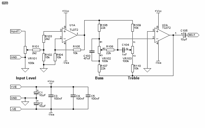
The mixer is the common "virtual earth" mixing amplifier, and there is nothing special about it. Note that it is inverting, which complements the tone controls (also inverting) so the absolute signal polarity is maintained. As shown, the mixer...
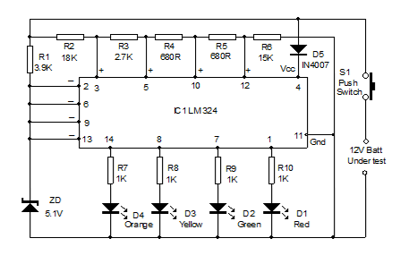
Battery Volt Meter Circuit Diagram. This circuit is designed to monitor the voltage level in Lead Acid or Tubular batteries. It provides four LED indicators to represent the voltage levels ranging from 9 volts to 14 volts. The battery voltmeter...
Automatic power switch for ATX power supplies. Visit the page to read the explanation about the related circuit diagram. The automatic power switch for ATX power supplies is a circuit designed to manage the power-on and power-off states of an...