
Low-Cost Prototyping For VHF Circuits

The passive VHF low-pass filter described operates effectively within the designated frequency range, leveraging a seven-pole configuration to achieve a minimal passband ripple of 0.003 dB at the specified cutoff frequency of 74 MHz. The choice of 50-ohm source and load impedances is standard for RF applications, ensuring compatibility with typical RF equipment. The microstrip design approach allows for a compact and efficient layout, utilizing a single-clad vector board that supports the necessary conductor and ground patterns.
The construction process employs copper-foil shielding tape, which provides flexibility in creating the microstrip conductor pattern, and the use of an epoxy-glass substrate ensures durability and stability of the filter. The soldering techniques applied to the inductors and capacitors are crucial for maintaining signal integrity and minimizing parasitic effects. The reduction of turns in the exterior inductors is a strategic decision aimed at improving performance by decreasing stray inductance, which is particularly important in high-frequency applications.
Comparative analysis of computed versus measured responses is essential for validating the filter's performance, and achieving a good correlation indicates successful design implementation. The consideration of unloaded Q factors further informs the selection of components, ensuring that the filter operates efficiently without excessive losses.
In production scenarios, transitioning to surface-mounted chip components and etched patterns can streamline manufacturing processes, reduce costs, and enhance reliability. The potential for a tubular filter design offers additional versatility for applications requiring different form factors or installation constraints. As the frequency approaches the UHF range, careful attention must be paid to connector types and substrate materials to maintain performance and address microstrip discontinuities effectively.Below 10 MHz, the realization of engineering models is fairly straightforward and not critically dependent on pc-board layout. At VHF, parasitic circuit elements and spurious coupling can wreak havoc with attempts to achieve performance at low cost without design iterations.
In this article, a passive VHF low-pass filter is presented that can be q uickly designed, constructed, and tested. The techniques discussed also apply to active circuits. The seven-pole low-pass filter has been designed for a passband ripple of 0. 003 dB at a nominal 3-dB cutoff frequency of 74 MHz ( Fig. 1 ). The source and load impedances are 50 ©. The circuit elements are shown in Table 1. The low-pass filter was constructed on a microstrip transmission line on a single-clad vector board. The vector board is mounted on male/female spacers in a Bud CU-123 die-cast aluminum box. The input and output connectors are Pomona 2451 BNC panel jacks. The vector board uses a 0. 062-in. thick epoxy-glass substrate with a hole grid of 0. 1 in. The microstrip conductor pattern is obtained using copper-foil shielding tape ( Fig. 2 ), which can be cut using scissors and an Xacto knife. The microstrip ground pattern uses the copper-clad side of the vector board ( Fig. 3 ). Filter components are soldered to the conductor and ground patterns in different ways. The interior inductors L3 and L5 are soldered to the conductor pattern via surface mounting. The exterior inductors L1 and L7 have one lead surface-mounted to the conductor pattern, while the other lead is soldered to the BNC connectors. To effectively absorb stray lead inductance, the number of turns for L1 and L7 has been reduced from six to five (all toroids are from Micro Metals).
The shunt capacitors C2, C4, and C6 each have one lead surfacemounted to the conductor pattern. The other lead of each capacitor passes through the substrate and is soldered to the ground pattern. When comparing the computed and measured amplitude responses (Table 2) for the low-pass filter, it can be observed that a reasonable correlation was obtained. The unloaded Qs of the inductors are approximately 100. The dissipation in the capacitors has been neglected. For production units, the low-pass filter would probably employ surface-mounted chip components with etched conductor patterns.
The low-pass filter also can be realized as a tubular filter. As the filter frequency approaches the UHF range, different connectors, different substrates, and etched components need to be employed. These connectors would provide microstrip launchers and all microstrip discontinuities will need to be addressed.
🔗 External reference
Related Circuits
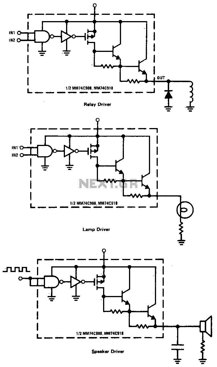
CMOS drivers for relays, lamps, speakers, and similar applications provide extremely low standby power consumption. When operating at Vcc = 15 V, the power dissipation per package is typically 750 nW when the outputs are not drawing current. Consequently,...
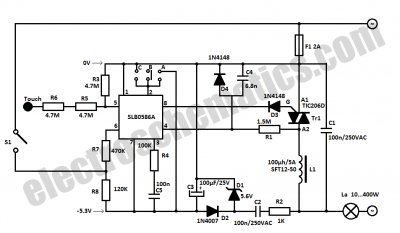
This light dimmer control features active timing capacitor reset or AC line zero-crossing synchronization. The 13 additional components are common and cost less than $2. Performance at the low end is exceptionally smooth and snap-free, even better than the...
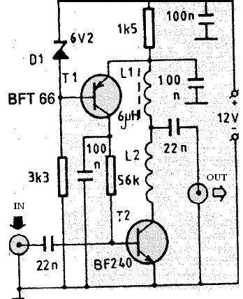
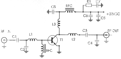
The PCB of this circuit should be positioned close to the antenna within a compact metallic enclosure. This VHF antenna circuit requires a 12 volts DC power supply, which can be sourced from a 12-volt battery, as the current...
At the beginning of the design process, the designer must determine which circuit structure is appropriate for a specific purpose. During this phase, numerical and symbolic analysis are of limited utility. There are no numerical values available for conventional...
If the audio input is a microphone, it is expected to precede an amplifier to achieve an output power of approximately 8W. The amateur seeking to enhance a small transmitter, which is likely already constructed, can utilize this circuit,...
The light fader circuits described here share a common concept of creating a gradual "cool" switch ON and switch OFF effect for connected lamps. This means that each time the lights are activated, the result is a smooth transition...