
Low-Cost Window Comparator
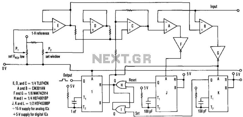
The circuit operates by utilizing a combination of operational amplifiers and comparators to create a robust signal processing system. The two potentiometers allow for fine-tuning of the reference voltages, providing flexibility for various applications. The operational amplifiers (A and B) serve as voltage comparators, comparing the incoming signal against the established reference levels. The use of a non-inverting summing amplifier (C) to derive the higher reference voltage is critical for establishing the acceptance window, which determines the thresholds for signal detection.
The Schmitt triggers (F and G) play a vital role in ensuring clean transitions between high and low states, effectively filtering out noise from the comparator outputs. This feature is particularly important in environments where signal integrity is paramount. The use of monostable multivibrators (J and K) allows for precise timing control, enabling the circuit to respond accurately to the changes in input signal conditions. The bistable latch formed by the NOR gates adds another layer of control, ensuring that the circuit behaves predictably during state changes.
Overall, this circuit is well-suited for applications requiring precise signal detection and processing, such as in communication systems, sensor interfaces, or data acquisition systems. Its ability to handle a range of frequencies and amplitudes makes it a versatile solution for various electronic design challenges. Modifications can be implemented easily to adapt to different operational parameters, further enhancing its utility in diverse applications. This circuit outputs a TTL-compatible - pulse whenever the signal falls within the limits set by potentiometers and can be varied to suit the application. Op amps, E, D, and C are used with the two potentiometers to supply reference voltages, derived from a 1-V precision source, for two other op amps (A and B) configured as voltage comparators. The input signal is taken to the negative inputs of both these comparators. C is wired as a noninverting summing amp, used to derive the higher reference voltage. Consequently, the acceptance window is set. Because the voltage across potentiometer P2 is 0.5 V, the window can be set between 0 and 0.5 V above the value chosen for the lower reference value.
The lower value is set by PI. The outputs from the comparators are sent to the inputs of inverting Schmitt triggers F and G. Although these triggers operate from a 5-V supply, they have an extended input-voltage range and are capable of handling the comparator"s output voltage swings. The two monostables, J and K, are triggered on the rising edge of the Schmitt outputs. J and set and reset the bistable latch formed by two NOR gates. Latch output Q controls the reset of output monostable L, which can only be triggered if its input goes low, taken from the output of G, while its reset is high.
From the timing diagram, when the signal input exceeds the lower reference level, the latch is set and Q goes high. When the higher reference level is exceeded, the latch is reset and Q goes low. If only the lower reference is exceeded, the latch will be set and L is triggered when G"s output goes low.
When both levels are exceeded, the latch is set, then reset. When G"s output goes low, it won"t trigger the mono-stable because its reset is low. The circuit, as shown, was used for a bandwidth-limited, 500- to 5 000 Hz input signal with an amplitude range of ± 1 V. Modifications can easily be made to cover other frequency and amplitude ranges. 🔗 External reference
Related Circuits
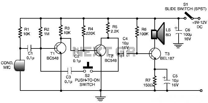
This is a low-cost and simple intercom circuit design. Some intercom circuits are built using integrated circuits. The circuit described here utilizes three readily available transistors that can be easily found in electronic stores. Even a novice can assemble...
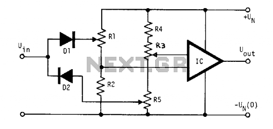
The voltage to be compared is fed through diodes D1 and D2 to the voltage dividers R1 and R5, where the low and high limits are established. When the input signal voltage exceeds the high threshold limit set with...

This circuit features independently adjustable upper and lower threshold settings, with digital outputs indicating the sign, within the window range, for both the upper and lower thresholds. The circuit utilizes two integrated circuits (ICs): the LM319 and the TL081. The...
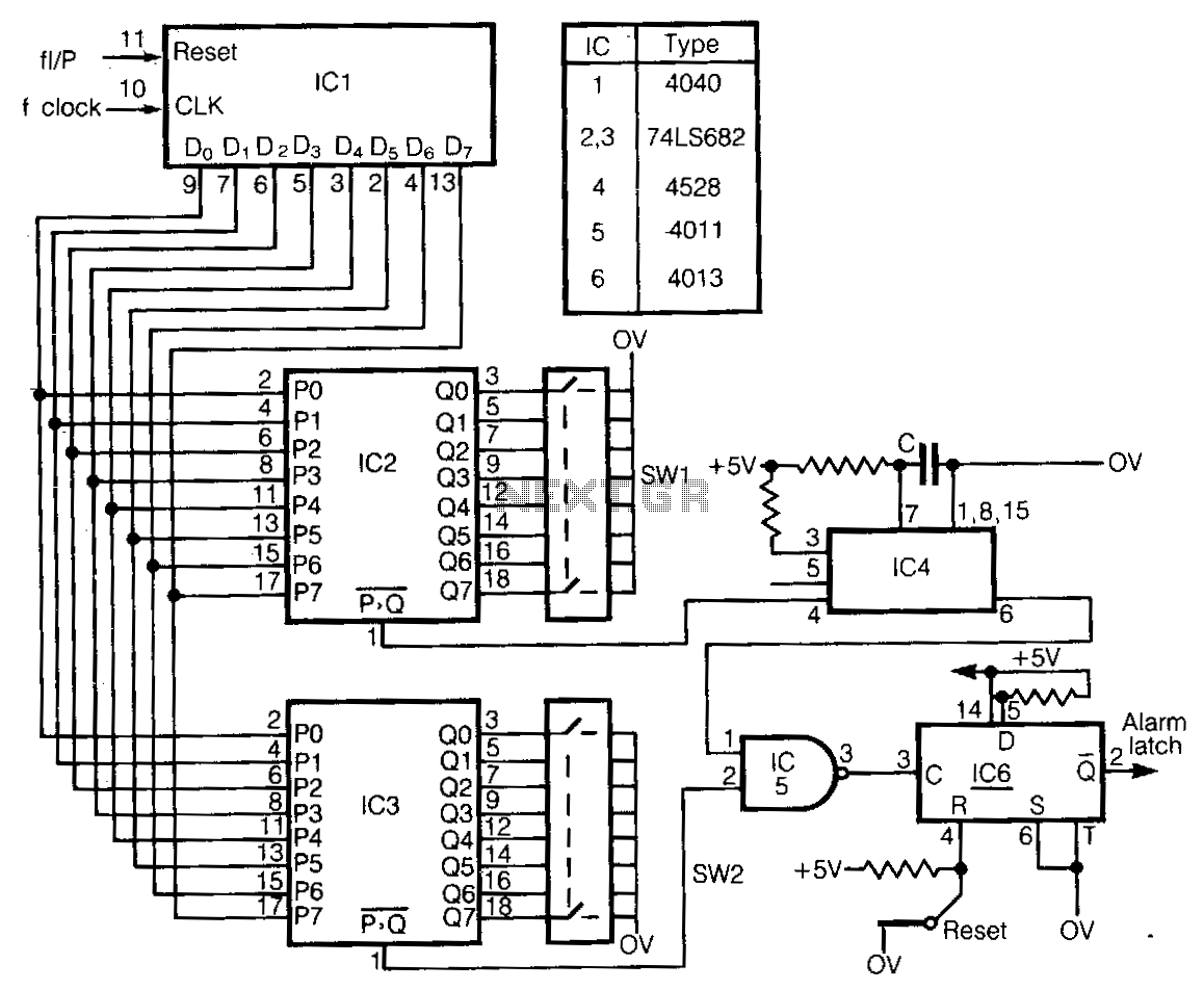
This circuit detects frequency variations that exceed preset limits. IC1 functions as a binary counter connected to the clock frequency (FcLK). The outputs from IC1 are compared with preset values set by IC2 and IC3. The input signal, which...
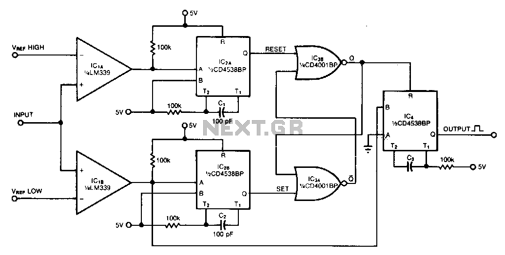
This window comparator generates an output pulse for each event that occurs within a specified window. Each output pulse signifies an input voltage pulse or level change that exceeds VREFLOW but not VREFHIGH. The monostable multivibrators, IC2A and IC2B,...

These two comparators function as over-voltage and under-voltage comparators. In the first configuration, if the measured voltage (Vm) exceeds the reference voltage, the output of IC1 goes low. In the second configuration, if the input voltage (ViN) exceeds the...
Warning: include(partials/cookie-banner.php): Failed to open stream: Permission denied in /var/www/html/nextgr/view-circuit.php on line 713
Warning: include(): Failed opening 'partials/cookie-banner.php' for inclusion (include_path='.:/usr/share/php') in /var/www/html/nextgr/view-circuit.php on line 713