
Low Frequency Sine wave Generators Schematic
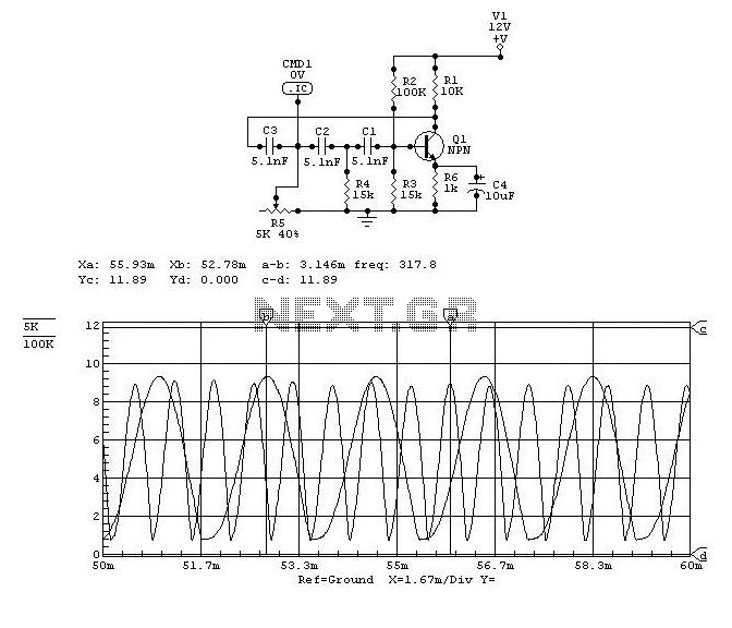
The described circuit employs two distinct methods for generating low-frequency sine waves, utilizing phase-shifting techniques through RC networks. The first method, utilizing a transistor circuit, involves a 3904 transistor which serves as the primary amplification stage. This circuit requires careful tuning of the 500-ohm resistor to optimize gain and minimize distortion, which can be a challenging task, limiting its practicality for general applications. The output from the collector is buffered by a JFET to ensure low output impedance, which is essential for driving subsequent stages.
The second method, based on an operational amplifier (op-amp), offers a more robust solution for generating sine waves. The op-amp configuration allows for a higher gain setting, which can be adjusted to maintain oscillation stability. The output taken from the RC network effectively filters out unwanted harmonic components, resulting in a cleaner sine wave. The specified values of 7.5K ohms and 0.1 microfarads create an oscillation frequency of approximately 600 Hz. Adjusting the resistor values proportionately can lower the frequency as needed.
The feedback loop established through the 7.5K resistor connected to pin 2 of the op-amp is crucial for controlling the gain of the oscillator circuit. This resistor is chosen to ensure that the output at pin 1 experiences slight clipping at its peaks, which is a desirable characteristic for maintaining waveform integrity. The final sine wave output, measured at pin 7, achieves a peak-to-peak voltage of about 5 volts when powered by a 12-volt supply. The clean appearance of the output on an oscilloscope confirms the effectiveness of the RC network in minimizing distortion, making the op-amp-based phase shift oscillator a superior choice for applications requiring stable sine wave generation.The two circuits below illustrate generating low frequency sine waves by shifting the phase of the signal through an RC network so that oscillation occurs where the total phase shift is 360 degrees. The transistor circuit on the right produces a reasonable sine wave at the collector of the 3904 which is buffered by the JFET to yield a low impedanc
e output. The circuit gain is critical for low distortion and you may need to adjust the 500 ohm resistor to achieve a stable waveform with minimum distortion. The transistor circuit is not recommended for practical applications due to the critical adjustments needed.
The op-amp based phase shift oscillator is much more stable than the single transistor version since the gain can be set higher than needed to sustain oscillation and the output is taken from the RC network which filters out most of the harmonic distortion. The sine wave output from the RC network is buffered and the amplitude restored by the second (top) op-amp which has gain of around 28dB.
Frequency is around 600 Hz for RC values shown (7. 5K and 0. 1uF) and can be reduced by proportionally increasing the network resistors (7. 5K). The 7. 5K value at pin 2 of the op-amp controls the oscillator circuit gain and is selected so that the output at pin 1 is slightly clipped at the positive and negative peaks. The sine wave output at pin 7 is about 5 volts p-p using a 12 volt supply and appears very clean on a scope since the RC network filters out most all distortion occurring at pin 1.
🔗 External reference
Related Circuits

A circuit is being designed that utilizes a combination of switches and resistors to enable a microcontroller to identify which switch has been pressed based on the voltage read, and subsequently perform a switch-specific action. The proposed design incorporates...
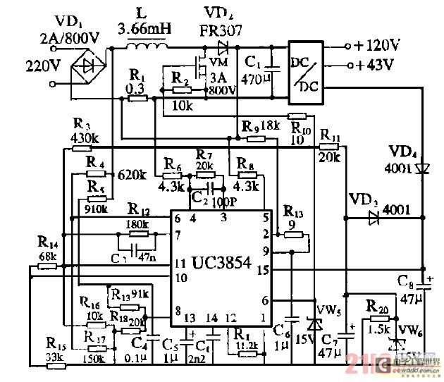
Improve the power factor (PF) to enhance energy conservation in electrical equipment. With advancements in electronic technology, high-frequency active power factor correction (PFC) technology has been increasingly applied across various power systems. The switching power supply of large-screen color...

A simple circuit that can generate an inverted square wave similar to the one used by the inventor on his function generator. To construct a circuit that produces an inverted square wave, a basic approach involves using a 555 timer...
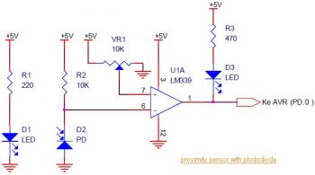
This circuit diagram illustrates a Line Follower / Line Tracker robot. The circuit is derived from tutorial documentation, which is available for download at the conclusion of this article. The line follower robot utilizes eight proximity sensor modules. Each...
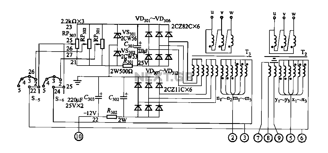
FGDF-3 is a three-phase low-temperature iron plating power supply circuit, while the KGDF-3 is a single-phase low-temperature iron plating power supply device that encompasses all the characteristics of the power supply unit. This design allows for an even distribution...
This is a convenient design for a transistor tester. The advantage of this circuit is that transistors can be tested without actually doing the circuit soldering. The tester uses two ICs: an NE 555 timer and a CMOS IC...