
Low-Level Power Fet Driver Method
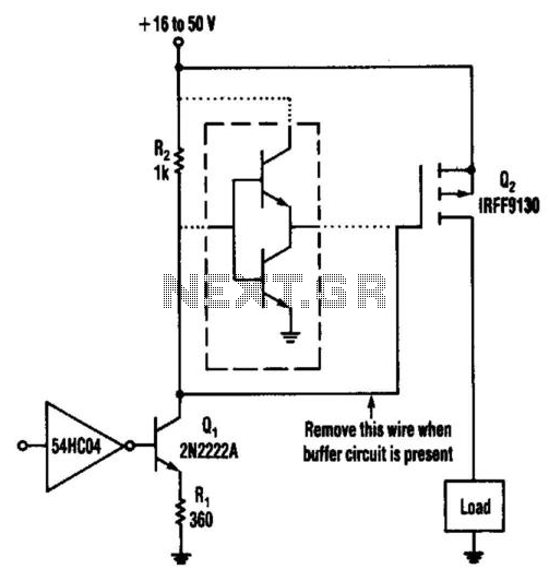
This circuit is designed to operate within a voltage range of 16 to 50 volts, making it versatile for various applications. The inclusion of a buffer circuit, indicated within the dashed lines in the schematic, enhances the performance by achieving switching times as low as 100 nanoseconds. In its standard configuration, the circuit achieves a switching time of approximately 1 microsecond, which is adequate for many applications but can be improved.
The core of the circuit consists of a transistor (Q1) and a resistor (R1), which together function as a switched current source. This current source is capable of delivering around 12 milliamperes (mA) to the load. The current then passes through another resistor (R2), which regulates the voltage supplied to the field-effect transistor (FET) at 12 volts. This configuration allows the circuit to maintain stable operation across a broad spectrum of supply voltages, ensuring reliable performance even in the presence of significant voltage ripple and noise.
To optimize the switching time, it is possible to reduce the values of resistors R1 and R2. However, this modification comes with a trade-off, as it results in increased power dissipation within both the resistors and the transistor Q1. Therefore, careful consideration must be given to the thermal management of these components when adjusting their values.
Alternatively, the implementation of a buffer circuit can significantly enhance the switching speed to 100 nanoseconds while maintaining low power dissipation levels. This is particularly advantageous in applications where rapid switching is critical, and power efficiency is a concern. Overall, this circuit design provides a robust solution for applications requiring reliable switching performance across varying supply conditions. This circuit operates from a 16- to 50-V supply. Adding the buffer circuit (within the dashed lines) offe rs 100-ns switching times. Otherwise, the circuit switches in 1 /xs. Ql and R1 form a switched current source of about 12 mA. The current flows through R2, which supplies 12 V to the FET. The circuit works well over a wide range of supply voltages. Furthermore, it switches smoothly in the presence of large ripple and noise on the supply. The switching time (about 1 /as) can be reduced considerably by lowering the values of Ri and R2 at the expense of higher power dissipations in the resistors and Ql. Alternatively, a buffer circuit can be added to produce switching times of 100 ns without generating significant power dissipation.
🔗 External reference
Related Circuits
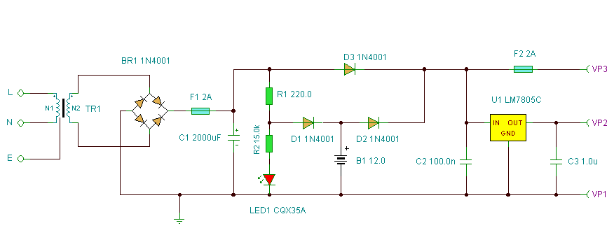
This circuit is a simplified version of a commercial uninterruptible power supply (UPS). It provides a constant regulated output of 5 volts and an unregulated supply of 12 volts. The described circuit functions as a basic uninterruptible power supply, designed...
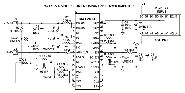
The IEEE 802.3af standard defines the interaction between power-sourcing equipment and powered devices within a power-over-Ethernet system. The IEEE 802.3af standard, also known as Power over Ethernet (PoE), specifies the mechanisms by which electrical power is transmitted alongside data over...
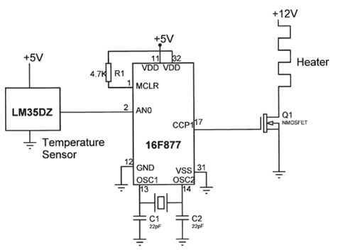
The electrical circuit diagram of this temperature control circuit consists of a 3-pin analog temperature sensor (LM35DZ), a built-in A/D converter microcontroller (PIC16F877), and the heater driver (IRL1004). The temperature control circuit utilizes the LM35DZ, a precision analog temperature sensor...
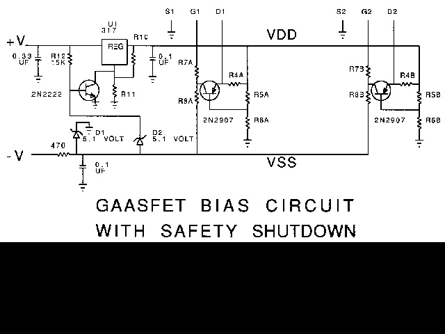
WB5LUA described GaAsFET preamplifiers for several microwave bands, which included an active bias circuit for the GaAsFET. Although newer devices have been introduced that offer improved performance, they require different bias points with varying currents and voltages. Modifying the...
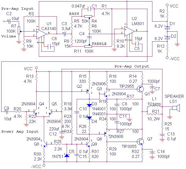
The circuit power amplifier depicted is a schematic design for a power amplifier with an output power of 70 watts, operating in Class AB mode. This power amplifier circuit is equipped with a tone control circuit. The 70-watt power...
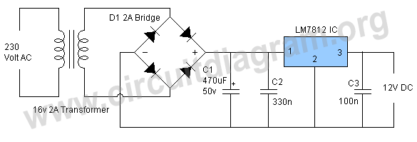
This project involves a straightforward and practical 12V power supply circuit utilizing the LM7812 integrated circuit (IC). The LM7812 is a three-terminal fixed voltage regulator IC housed in a TO-220 package. It incorporates several built-in features such as thermal...