
Low Power consumption 5V regulator circuit
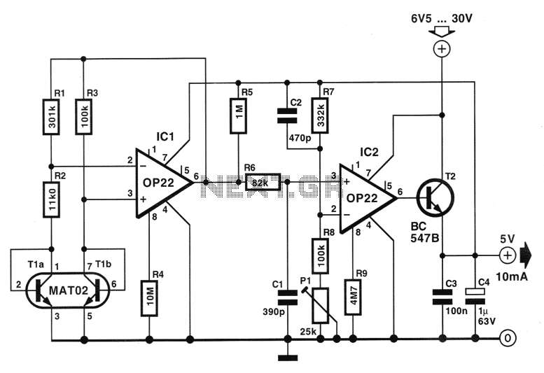
In cases where these specific transistors are hard to find, two common BC transistors can be used, provided they are selected to have approximately the same threshold voltage. The operational amplifiers IC1 and IC2 are of the OR22 type. For IC2, the peak output current can be adjusted by varying the input power through resistor R9. The input current can range from 400 mA to 500 mA. Before increasing the current, it is essential to verify that the output transistor T2 can handle the higher currents that may be demanded by the load. The filter formed by resistor R6 and capacitor C1 is intended to suppress any unwanted peaks that may inadvertently appear at the input of IC2. Capacitor C2 enhances the stability of the circuit, particularly when the stabilizer is required to deliver pulsed current. The overall circuit resistance is highly sensitive to electrostatic and magnetic disturbances.
The control stabilizer is designed with a complex load to draw a continuous current of 1 mA. Measurement results for the 1 mA pulse are recorded in the accompanying table. The current Ig represents the quiescent current of the stabilizer.
The circuit's design emphasizes efficiency and stability, making it suitable for applications where low power consumption is critical. The choice of transistors and operational amplifiers is crucial for maintaining the performance of the voltage regulator. The use of matched transistors helps to ensure consistent behavior under varying load conditions, which is particularly important for maintaining the desired output voltage. The inclusion of filtering components further enhances the circuit's immunity to noise, thereby improving its reliability in practical applications. Overall, this circuit represents a compact solution for effective voltage regulation with minimal power draw.The special feature of the circuit shown below is the low consumption. With voltage n 9 at the entrance and no exit load, absorbs current 50 ma, which is certainly very small compared with a quiescent current 78L05. The components that comprise it are scarce. Just a reference voltage source, formed by the T1 and the IC 1 and an amplifier consisting of the IC2 and T2 so we have to output the desired voltage stabilizer.
The trend that emerges at the output of IC 1 increased to 1,22 V. Using the IC2 and the P1 is set so that the output of the circuit is n equal to 5 exactly at the entrance of the circuit can be imposed voltage between 6.5 ??? 30 V DC, while the maximum output current reaches 1 mA for the better functioning of the stabilizer, transistors T and T 1 a 1 b should be possible similar characteristics.
That is why we preferred a 'double' type transistors MAT02 or alternatively one of the MAT01, SSM2210 or LM394. If your course is hard to find, you can use two common BC, but which should be selected to have approximately the same threshold voltage. The Operational IC 1 and IC2 is type OR22. Especially for IC2, the peak current of the output can be set using the power introduced in this through the resistor R9.
The price of electricity varies between 500 to 400 ma BAC course, before making an increase, you should check whether the output transistor T2 is able to meet the equally elevated currents that it may request the load. The filter formed by the R6-C 1 is meant to suppress the spurious peaks may accidentally be deployed at the entrance of IC2.
The capacitor C2 improves the stability of the circuit, wherethose which the stabilizer is required to provide pulsed current. The total circuit resistance and is highly therefore sensitive to any kind of electrostatic and magnetic disturbances.
The control stabilizer made with a complex load to absorb continuous stream of 1 mA. The pulse of 1 mA Measurement results are shown in the table. The current Ig represents the quiescent current of stabilizer. 🔗 External reference
Related Circuits

This circuit displays three voltage levels: normal (11 to 15 V), high (greater than 15 V), and low (below 11 V). When the voltage is low, the LED illuminates steadily. In the normal voltage range, the LED remains off....
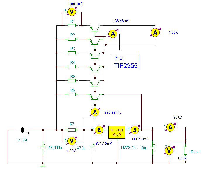
This power supply utilizes a single 7812 integrated circuit (IC) voltage regulator in conjunction with multiple external pass transistors to provide output load currents of up to 30 amps. The circuit design incorporates a 7812 voltage regulator, which is known...
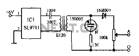
The electronic frostbite treatment instrument ASIC SL9711 consists of an oscillation circuit, a power amplifier, and a controller. It generates a sine wave at frequencies of 100 Hz and 3 Hz, followed by a step-up transformer with potentiometer adjustment...
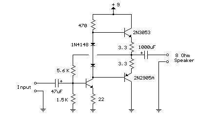
This weblog focuses on electronic circuit schematics, PCB design, DIY kits, and electronic project diagrams. The following describes a small audio amplifier, similar to those found in medium-sized transistor radios. The input stage is biased to ensure equal power...
A functional circuit utilizing an operational amplifier (op-amp); however, the instructor indicated that op-amps can be challenging to work with and provided transistors as an alternative. Operational amplifiers (op-amps) are versatile components commonly used in various electronic circuits for...
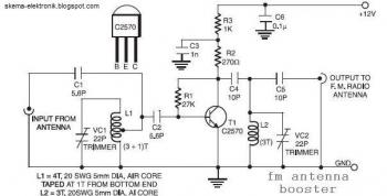
The input coil L1 is composed of four turns of 20 SWG enamelled copper wire, wound slightly spaced over a 5 mm diameter former. It is tapped at the first turn from the ground lead side. Coil L2 is...