
Active FM Antenna Booster circuit
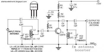
The circuit features two inductors, L1 and L2, which are critical components in the FM antenna booster design. L1, with four turns, is designed to provide a certain inductance value that enhances the input signal. The use of 20 SWG enamelled copper wire ensures good conductivity and minimizes losses due to resistance. The slightly spaced winding technique may be employed to reduce the coupling between the turns, which can help in tuning the circuit's resonant frequency.
Coil L2, having three turns, serves a similar function but may be tailored for a different frequency or gain requirement. The difference in the number of turns between L1 and L2 allows for fine-tuning of the circuit's performance characteristics. The tapping of L1 at the first turn from the ground lead side indicates that this point may be used for feedback or signal extraction, which is essential for maintaining stability and enhancing the overall gain of the amplifier.
The transistor 2SC2570 is a key active component in this circuit, and its pin configuration is crucial for proper integration into the schematic. This transistor is typically used in RF applications due to its favorable frequency response and gain characteristics. The configuration must be adhered to ensure that the transistor operates within its optimal range.
Adjustable trimmers VC1 and VC2 are included in the design to allow for precise tuning of the input and output stages of the amplifier. By manipulating these trimmers, the user can achieve maximum gain, which is vital for effective signal amplification in an FM antenna application. Proper adjustment ensures that the circuit operates efficiently, minimizing distortion and maximizing signal clarity.
Overall, this schematic emphasizes the importance of component selection and configuration in achieving optimal performance in an FM antenna booster circuit.Input coil L1 consists of four turns of 20SWG enamelled copper wire (slightly space wound) over 5mm diameter former. It is tapped at the first turn from ground lead side. Coil L2 is similar to L1, but has only three turns. Pin configuration of transistor 2SC2570 is shown in the fm antenna booster schematic. Adjust input/output trimmers (VC1/VC2) for maximum gain. 🔗 External reference
Related Circuits
This circuit dials a stored DTMF tone sequence from an EPROM when a control line is taken to 0 V. IC1 is a Schmitt trigger oscillator, operating at approximately 2 Hz. It clocks a 4024 binary counter. The outputs...
The PCB of this circuit should be positioned close to the antenna within a compact metallic enclosure. This VHF antenna circuit requires a 12 volts DC power supply, which can be sourced from a 12-volt battery, as the current...
Most universal radio receivers have a very wide bandwidth that is not particularly suitable for radio amateurs. The better models with narrower bandwidth are almost a... Universal radio receivers are designed to operate over a broad frequency range, making them...
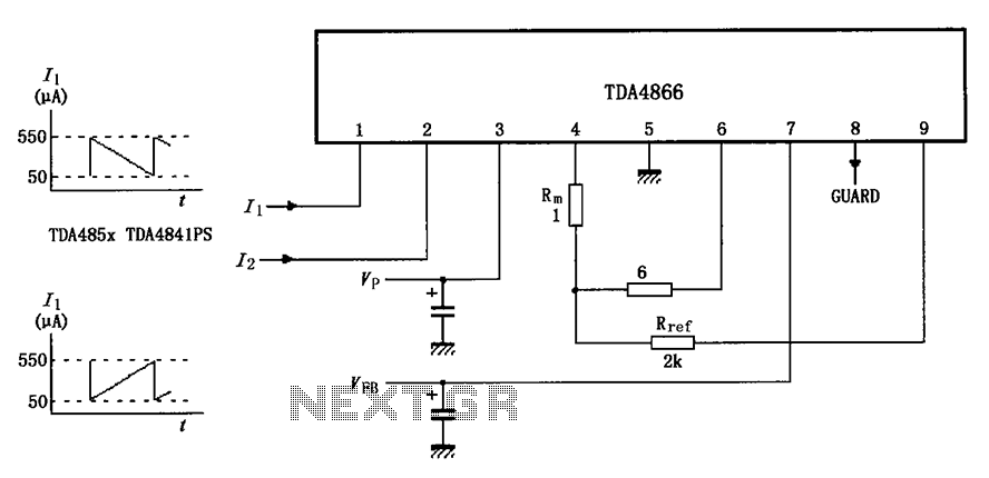
The TDA4866 test circuit operates with a positive supply voltage (VP) and a feedback voltage (VFB) in conjunction with a flyback circuit. The circuit responds to changes in the input signal, transitioning from one state to another. The input...
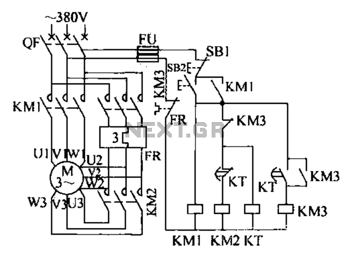
The extended delta decompression starter is designed to manage the operation of a three-phase motor during startup. It involves the initial connection of the motor's three-phase winding set to facilitate a reduced voltage startup, which is achieved through a...
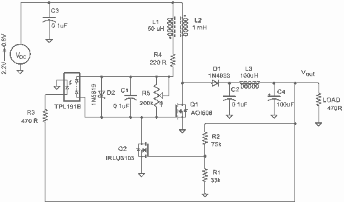
It employs a low threshold MOSFET and two coupled coils to function as a joule thief. An additional MOSFET is utilized for regulation. The circuit operates as a joule thief, which is a type of DC-DC converter designed to extract...
Warning: include(partials/cookie-banner.php): Failed to open stream: Permission denied in /var/www/html/nextgr/view-circuit.php on line 713
Warning: include(): Failed opening 'partials/cookie-banner.php' for inclusion (include_path='.:/usr/share/php') in /var/www/html/nextgr/view-circuit.php on line 713