
low side mosfet drive circuits and 23

A low-side switch is defined as a configuration where the MOSFET sinks current, with the load positioned between the drain and the positive voltage supply. The source connects to ground, and the gate is driven relative to ground. Focusing on N-channel Power MOSFETs, it is crucial to note that these devices are fully activated when the gate-to-source voltage (VGS) exceeds 8V. While the MOSFET can operate with VGS above the threshold voltage (VGS(threshold)), it will not be fully turned on at voltages below 8V, resulting in operation within the linear region and significant power losses.
In contrast, Logic Level MOSFETs generally have lower VGS(threshold) values, allowing them to be fully activated with VGS levels between 4V and 5V. However, a drawback of Logic Level MOSFETs is their typically higher on-state resistance compared to similarly rated Power MOSFETs, which can lead to increased conduction losses for the same load.
Gate capacitance is another critical consideration. To turn the MOSFET on or off, the gate must be driven high or low with sufficient current to charge or discharge the gate capacitance quickly. This rapid switching minimizes the time the MOSFET spends in the linear region, which is particularly important for high-speed switching applications. In low-frequency scenarios, the time spent in the linear region may not be as significant, as the MOSFET will be fully on for the majority of the time.
In a basic application where a MOSFET drives a load and is periodically turned on and off, the duration of these cycles can vary significantly based on the specific application. For instance, a MOSFET might control a DC fan that operates for two hours and then remains off for an hour, cycling on and off at longer intervals. In such cases, the drive strategy is straightforward: applying a sufficient voltage to the MOSFET gate turns it on, while grounding the gate turns it off. Although rapid charging and discharging of the gate capacitance is always favorable, it may not be critical in low-frequency applications due to the extended on and off durations.
In these circuits, Vin represents the input drive signal to the MOSFET, while +V_DRIVE is the voltage supply used to drive the MOSFET. When the MOSFET is on, VGS equals +V_DRIVE, and when it is off, VGS equals 0. Each MOSFET has a maximum rated VGS, typically around 20V for most devices, though some may reach up to 30V, and Logic Level MOSFETs often have lower maximum ratings. It is advisable to consult the specific MOSFET's datasheet for accurate ratings.
An example circuit is illustrated in Fig. 1, depicting an inverting driver configuration. In this setup, the MOSFET turns on when Vin is low and turns off when Vin is high, controlling the load accordingly.MOSFETs cannot always just be connected to the drive signal and be expected to work properly. Due to the construction of the MOSFET, driving it is not the simplest of tasks, especially for beginners. There are many users who regularly ask for help on MOSFET drive related issues or problems on different blogs, websites and forums.
So, here I will show some MOSFET drive techniques/methods for MOSFETs configured as low-side switches. Before I head on to MOSFET drive, let me just tell you what a low-side switch is, in case you don`t know. When the MOSFET (that you`re using as a switch) sinks current, it is a low-side switch. The load will be between the drain and +V supply. The source will be connected to ground. Gate will be driven with respect to ground. Let me start with N-channel Power MOSFETs. One thing to keep in mind is that these MOSFETs are fully turned on when the voltage at the gate with respect to the source (VGS) is > 8V.
So while at voltages less than 8V, the MOSFET will be on (as long as VGS > VGS(threshold) ), the MOSFET won`t be fully turned on. It will operate in the linear region and there will be very high losses. Now let`s go to Logic Level MOSFETs. These MOSFETs tend to have much lower VGS (threshold) and thus are usually fully turned on with VGS of 4V to 5V.
One downside to Logic Level MOSFETs is that they usually have higher on-state resistances compared to similarly rated Power MOSFETs. So, this would mean higher conduction losses for the same load. Another thing to remember is the gate capacitance. So, when the MOSFET is to be turned on or off, the gate must be driven high or low with sufficient current quickly enough so as to charge or discharge the gate capacitance quickly enough so that the MOSFET spends minimal time in the linear region and is quickly turned fully on or off.
This is true especially for high speed switching when time period is small. However, in low frequency applications, this may not be a big problem as, even if the MOSFET spends some time in the linear region, it will spend the (remaining) majority time fully on and thus the small amount of time spent in the linear region will not cause much of a problem. Let`s first consider the simplest situation: a MOSFET is driving a load and is periodically turned on and off to turn the load on and off respectively.
How long do I mean by periodically Well, it really depends on the application. But for this situation, the period between turning on and off may be very long or very short but will be at least half a second. A few examples: The MOSFET could be driving a DC fan that will be turned on, kept on for 2 hours and then kept off for about an hour and turned on and off in few hour intervals.
In such situations, MOSFET drive is simplest apply a high enough voltage to the MOSFET gate and the MOSFET will be on; ground the MOSFET gate and the MOSFET will be off. Quick charging and discharging of the MOSFET gate capacitance are always desirable. But in this situation, the charging and discharging need not be very quick as frequency isn`t high. In each of these circuits Vin is the input drive signal to the MOSFET. +V_DRIVE is the voltage supply to drive the MOSFET. When the MOSFET is on, VGS = +V_DRIVE. When the MOSFET is off, VGS = 0. MOSFETs have a maximum rated VGS. For most MOSFETs, this is 20V. For some it is higher up to 30V. There are MOSFETs (usually Logic Level) which have a lower maximum rated VGS. It is always best to check the datasheet for the specific MOSFET being used. Fig. 1 shows an inverting driver. Here, the MOSFET is turned on when Vin is low and turned off when Vin is high. When the MOSFET is on, the load is on and vice versa. In Fig. 🔗 External reference
Related Circuits
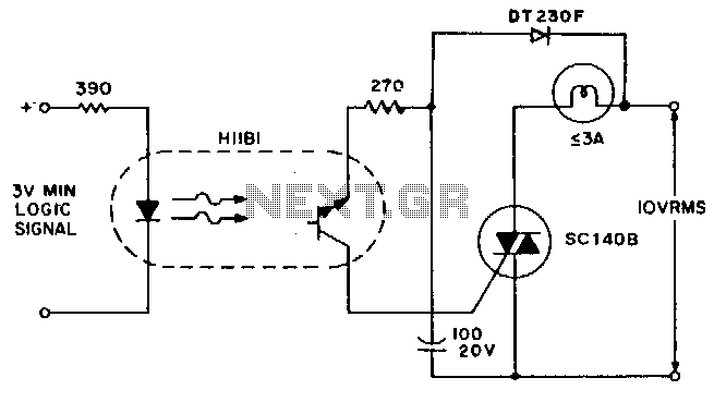
A simple solid-state relay circuit drives the 10-Vac telephone indicator lamps from logic circuitry while maintaining complete isolation between the 10-V line and the logic circuit. The described circuit utilizes a solid-state relay (SSR) to control 10-Vac telephone indicator lamps...
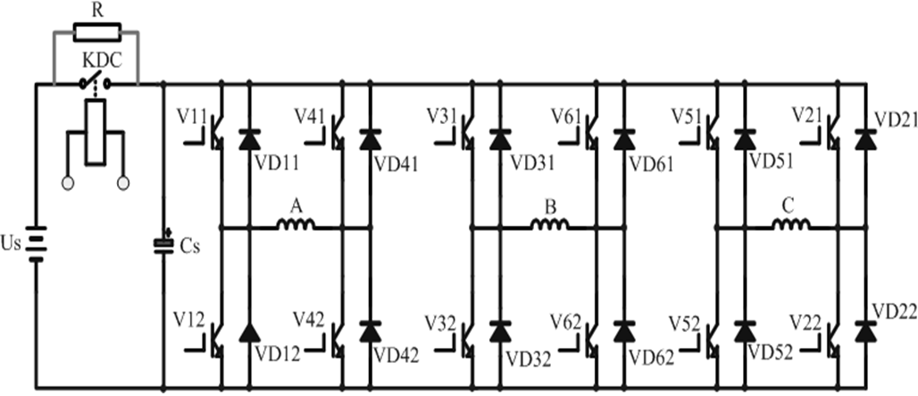
With the continuous growth of global vehicle production and ownership, the problems associated with vehicles are becoming increasingly apparent, particularly in China. Consequently, the development of zero-emission electric vehicles has emerged as a primary scientific research focus for many...
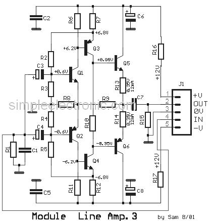
This is a simple low-impedance preamplifier circuit diagram used to amplify an audio signal. The circuit operates with a 12V DC power source and is straightforward due to its minimal component count. The low-impedance preamplifier circuit is designed to enhance...
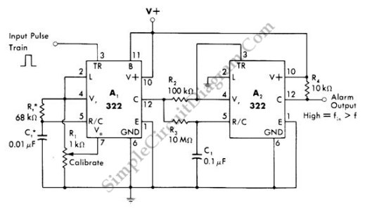
At high speeds, visually checking the speedometer to remain under the maximum speed can be hazardous. Implementing an audio alarm system would enhance safety by providing auditory alerts. To enhance vehicle safety at high speeds, an audio alarm system can...
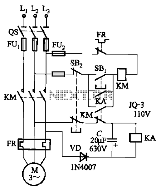
The circuit illustrated in Figure 3-73 is designed to utilize the power generated by instantaneous power failures, specifically the self-induced electromotive force (emf) produced by the motor, to implement an immediate shutdown protection mechanism. During a momentary power outage,...
This page outlines the development of electronics for displaying a monochrome video image on an electrostatic oscilloscope tube. This work complements the Electron Optics section in the Experiments category. The primary objective is to showcase a moving video image...