
RF Wireless Data Transfer communication Circuit diagram
The RF Wireless Data Transfer communication circuit utilizes radio frequency (RF) technology to establish a wireless link for transmitting data between two points. The core components of this circuit typically include a transmitter module, a receiver module, an antenna, and associated circuitry for modulation and demodulation.
The transmitter module converts the data signal into a radio frequency signal using modulation techniques such as Amplitude Shift Keying (ASK) or Frequency Shift Keying (FSK). The modulated RF signal is then transmitted through an antenna, which radiates the signal into the surrounding environment.
At the receiving end, the receiver module captures the RF signal using its antenna. The received signal is then demodulated to retrieve the original data. This demodulation process involves filtering and amplifying the signal to ensure that it is clean and free from noise. The output of the receiver module is then connected to a microcontroller or another processing unit, which interprets the received data for further action.
Power supply considerations are crucial in RF circuits, as both the transmitter and receiver require stable voltage levels for optimal performance. Additionally, the design may include features such as error detection and correction mechanisms to enhance the reliability of data transmission.
Overall, the RF Wireless Data Transfer communication circuit is designed for applications requiring short to medium-range data communication, making it suitable for various uses such as remote control systems, wireless sensor networks, and telemetry applications.RF Wireless Data Transfer communication Circuit diagram.we implemented a wireless communication interface one point to another by means of RF technology. 🔗 External reference
Related Circuits
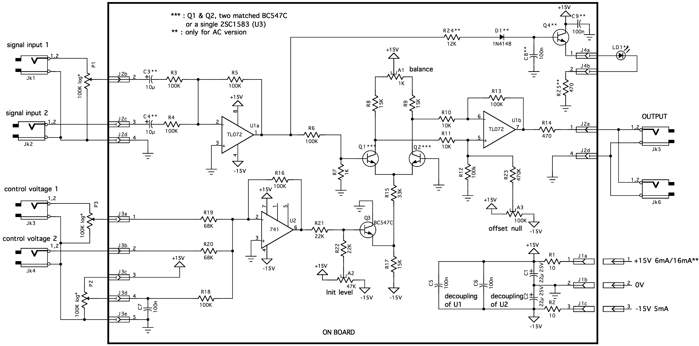
Trimming is straightforward when matched NPN transistors are utilized for Q1 and Q2, along with 1% tolerance resistors for R6 to R11. A dual trace oscilloscope, digital voltmeter (DVM), and sine wave generator are required for this process. Although...
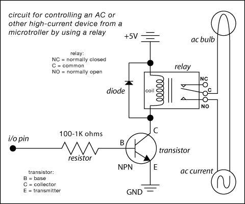
Here are some circuit diagrams for driving relays from a microcontroller. Ensure the use of a 5-volt relay (this refers to the coil, not the load circuit) and verify that the relay has a sufficient rating for the load...
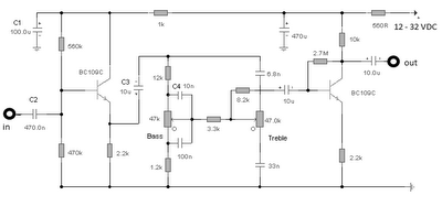
The first BC109C transistor functions as a buffer, delivering a high input impedance of approximately 250k and exhibiting a voltage gain marginally below unity. Given that the Baxendall tone control circuit operates passively, it attenuates all audio frequencies. The...
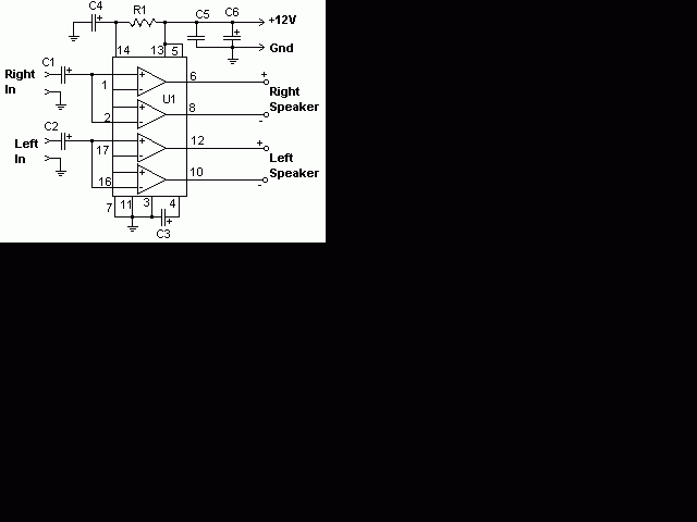
This is a stereo power amplifier circuit that operates at up to 22W per channel, resulting in a total output of 2x22W. A few external components are required to support the main component, the TDA1554. A heatsink on the...
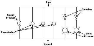
Each component of the circuit is represented in a simple block form with corresponding labels for identification, using no special symbols or language. The interconnections between these components are depicted by solid lines. The block diagrams can be read...
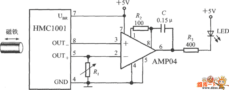
The image depicts a proximity switch circuit that includes the HMC1001 Hall effect sensor, an operational amplifier (AMP04), and a light-emitting diode (LED). In this configuration, the operational amplifier functions as a comparator. When a magnet with a length...