
0-1 hours of power a circuit diagram of the timing of the AC power supply
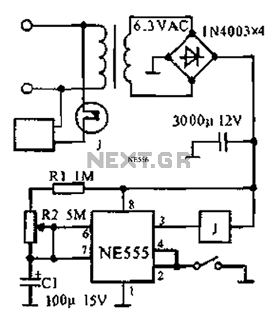
The circuit utilizes a 555 timer IC, which is widely recognized for its versatility in timing applications. In this configuration, the 555 timer is set up in monostable mode, meaning it generates a single output pulse when triggered. The duration of this pulse, which corresponds to the timer's delay, is governed by the time constant determined by the resistor R2 and capacitor C1.
The relay, specifically the J 212 IRC MR312C, is employed to switch AC loads. When the 555 timer is triggered, it energizes the relay coil, allowing current to flow through the relay contacts and subsequently activating the connected load. The specified coil current of less than 200 mA ensures compatibility with the 12V power supply, making it suitable for various applications.
For users seeking to modify the delay time, adjustments to the resistance of R2 or the capacitance of C1 will result in different timing intervals. The relationship between resistance, capacitance, and time delay can be described by the formula:
\[ T = 1.1 \times R \times C \]
Where T is the time delay in seconds, R is the resistance in ohms, and C is the capacitance in farads. By selecting appropriate values for R2 and C1, a wide range of timing options can be achieved, from the minimum of 3 minutes to the maximum of 58 minutes.
The pin configuration of the NE555 timer is crucial for proper operation. Pin 8 is connected to the positive supply voltage (VCC), while pin 1 is grounded. Pin 2 is the trigger input, which initiates the timing cycle when a low signal is applied. Pin 3 provides the output signal to control the relay, and pin 4 is connected to the reset pin to allow for manual resetting of the timer. Pin 6 serves as the threshold input, and pin 7 is the discharge pin that discharges the timing capacitor once the timing interval is complete.
This circuit design is ideal for applications requiring timed control of AC devices, such as lighting systems, motor controls, or any other equipment that necessitates a delay before activation. As shown when the power supply is 0 to 1 hour, set the AC circuit diagram 555 constituted within one hour timer, J 212 IRC MR312C relay coil impedance, or current of less than 200mA 12V relay. FIG parameters, the delay time is 3 to 58 minutes. If you want to get other time range, change the value of R2 and C1. Clockwise as seen from the top of the foot NE555R order 8,3,4,2,1,7 and 6.
Related Circuits
This circuit simulates a breathing or pulsing LED using a 555 timer chip. It has gained popularity, receiving numerous comments and emails from users who successfully built the circuit, as well as feedback from those who encountered difficulties when...
The IRF9540N Gate Charge Test Circuit is illustrated in the diagram below. The IRF9540N is recognized as a rectifier device that employs advanced processing techniques to attain an exceptionally low on-resistance per unit area, as stated in the datasheet....
The output frequency of this simple, low-cost active voltage-controlled oscillator circuit is based on the inherent frequency-dependent characteristics of an operational amplifier. The oscillator circuit utilizes a TL082 op-amp. Upon application of power, the circuit generates a sinusoidal wave....
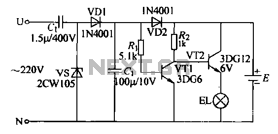
An automatic emergency lighting circuit is presented, suitable for self-installation in households. It utilizes smaller components, resulting in a lower cost. Under normal conditions, the 220V AC mains voltage is reduced by capacitor C1, and then processed through a...
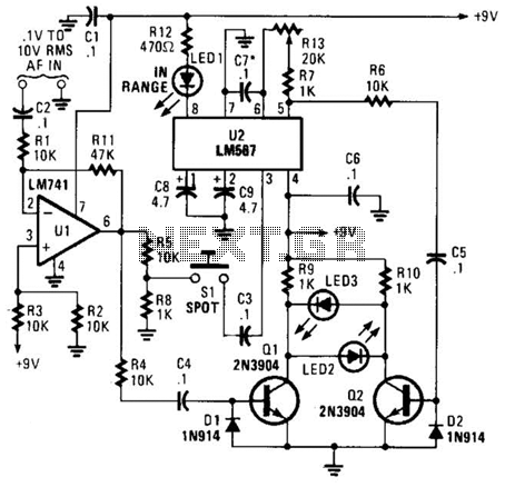
This meter is unique as it does not utilize a D'Arsonval movement or digital display for frequency readings. Instead, the measured frequency is indicated on a hand-calibrated dial. Any audio signal applied to the circuit is amplified by U1,...
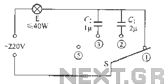
The capacitive dimmer switch circuit is illustrated in Figure 9. It operates based on the principle of capacitive reactance with alternating current. When the switch is in the position shown, the normal light bulb operates at maximum brightness. When...