
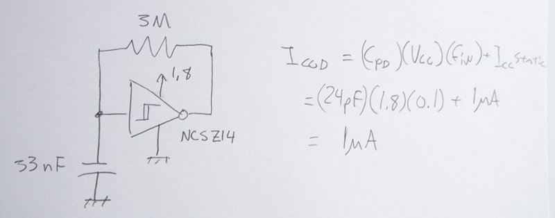
MAX668 inverting configuration quadruple pressure DC DC converter power supply

The described circuit employs the MAX868 in conjunction with CMPSH-3S to achieve a quadruple voltage output through a DC/DC conversion mechanism. The inverting charge pump configuration is particularly advantageous for applications requiring negative voltage supplies. The input voltage range of 1.8V to 5.5V allows for versatility in various electronic applications, ensuring compatibility with a wide range of power sources.
The pulse frequency modulation technique utilized by the MAX868 is effective in maintaining output voltage regulation while minimizing power loss, as evidenced by the low quiescent current of 30 µA, which contributes to overall energy efficiency. The maximum frequency of 450 kHz allows for rapid response to load variations, ensuring stable output under dynamic conditions.
The integration of capacitors C3 and C4 along with a Schottky diode in the feedback loop is crucial for the charge pump operation, enabling the generation of the desired quadruple voltage. The design allows for a maximum output voltage of -18V, which is suitable for various applications requiring negative voltage levels, such as operational amplifiers or analog signal processing circuits.
The current output capabilities of the circuit are noteworthy; the ability to provide 15 mA at -18V is complemented by the option to achieve higher current outputs at lower voltages, with 20 mA at -15V and 30 mA at -12V. This flexibility allows the circuit to adapt to different load requirements without compromising performance.
The feedback mechanism involving resistors R1 and R2 is fundamental in establishing the output voltage stability. The relationship VOUT = -VIN (R1/R2) ensures that the output voltage can be finely tuned by adjusting the resistor values, thus allowing for precise control over the output characteristics depending on the specific application requirements. Overall, this circuit design exemplifies a robust solution for generating stable negative voltages in compact electronic systems. As shown in FIG inverted to adopt IC1MAX868 and CMPSH-3S consisting of four times the pressure of DC/DC converter power supply. IC1MAX868 which is a type inverting charge pump regulator integrated circuit, can produce up to -2VIN output voltage, input voltage VIN range from 1.8 ~ 5.5V. IC1 through pulse frequency modulation (PFM) to regulate the output voltage, the maximum frequency of 450kHz.
Very low quiescent current (30 A). Insert a charge pump by the C3, C4 and Schottky diode in its feedback loop, to form a quadruple voltage inverter power supply circuit.The power supply at VOUT -18V, can provide current 15mA, efficiency 76%, ripple 60mV. If you reduce VOUT, allows a higher current output, such as when VOUT -15V, can provide 20mA, VOUT -12V when compared to 30mA.
Its stable output voltage by the feedback resistor Rl and R Ratio is determined. That VOUT -VIN (R1/R2).
Related Circuits
The power supply varies, and the circuit must operate at under 10 µA of current (excluding the capacitor charging). It triggers a Silicon Controlled Rectifier (SCR) every 10 to 30 seconds as long as the power supply is above...
This voltage-to-frequency converter is designed to connect to a frequency counter to display the measured voltage value. This converter-counter combination creates an inexpensive yet functionally complete digital voltmeter. The circuit outputs TTL-compatible pulses that are 5 µs wide. The...
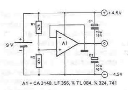
A symmetrical power supply can be designed using this circuit diagram. This symmetrical power supply is constructed with a simple operational amplifier and some classic electronic components. Resistors R1 and R2 form a high impedance voltage divider. The operational...
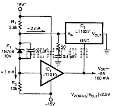
A method for enhancing the output current of a reference while also providing overload protection is illustrated. In this configuration, IC1 functions as a power buffer. The LT1027 regulates the output voltage (Vout) and ground to maintain a stable...
The Hewlett-Packard HSCH-3486 zero-bias Schottky diode is utilized as the detector. To avoid employing a modulation detection method, a chopper-stabilized operational amplifier is implemented. The chopper operational amplifier effectively converts the input DC voltage to AC, amplifies it, and...
The circuit consists of a series of dual power supplies, providing a symmetrical ±15V supply for linear circuits. The same principle is applicable to non-symmetrical supplies, such as 5.0V and -12V regulators, which are used in applications like registers....