
MC28332 Single Chip VHF Narrowband FM Transmitter Application Circuit
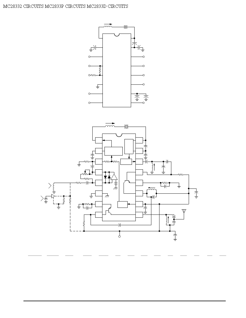
Crystal X1 is a critical component in RF transmitter designs, particularly in applications requiring precise frequency generation. Operating in fundamental mode, it ensures stable oscillation characteristics essential for maintaining signal integrity. The calibration for a 32 pF load capacitance allows for optimal performance, ensuring that the crystal resonates accurately at its designated frequency.
The MC2833 IC plays a pivotal role in the frequency multiplication process. It takes the fundamental frequency generated by Crystal X1 and multiplies it to achieve the desired output frequencies. The architecture of the MC2833 is designed to support various frequency multiplication techniques, enabling efficient signal processing within the transmitter.
The RF output buffer located at Pin 14 is essential for interfacing the output of the MC2833 with the subsequent stages of the transmitter circuit. This buffer amplifies the output signal, ensuring that it can drive the next stage without significant loss of power or signal quality. Additionally, the Q2 transistor is employed as a frequency doubler, effectively doubling the frequency of the output signal, while the frequency tripler configuration allows for the generation of higher frequencies, specifically at 76 MHz and 144.6 MHz.
In summary, the combination of Crystal X1, the MC2833 IC, and the associated RF output buffer and transistor configurations facilitates the generation of stable and precise RF signals, making it suitable for various communication applications, including amateur radio and other RF transmission systems.Crystal X1 is fundamental mode, calibrated for parallel resonance with a 32 pF load. The final output frequency is generated by frequency multiplication within the MC2833 IC. The RF output Buffer (Pin 14) and Q2 Transistor are used as a frequency tripler and doubler, respectively, in the 76 and 144. 6 MHz Transmitters 🔗 External reference
Related Circuits
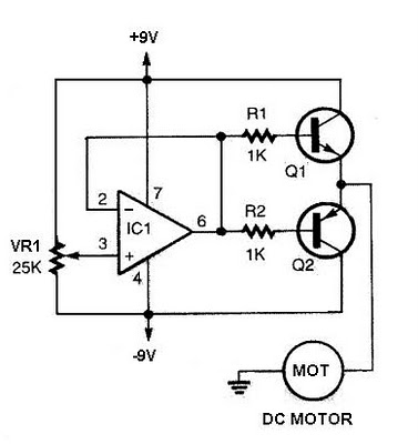
The speed increases in either direction as the potentiometer VR1 is adjusted toward its ends. The TIP3055 Q1 NPN power transistor has a collector current specification of 15A and a VCE0 rating of 60V DC. The MJE34 Q2 PNP...
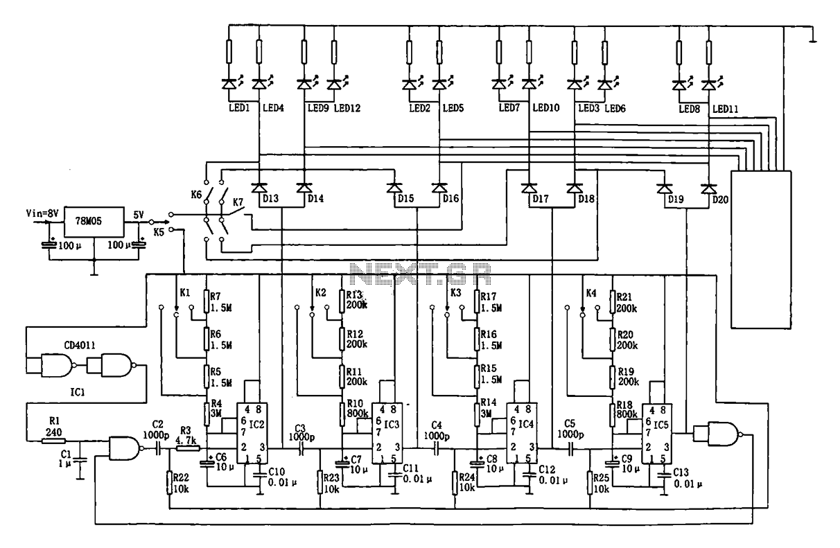
This document describes an automatic traffic intersection light control circuit. It features four monostable delay circuits, which consist of four 555 timer integrated circuits (IC2 to IC5) and several RC components interconnected. An 8V input voltage is regulated through...
Both circuits can synchronize trapezoidal wave voltage, which is converted into intermittent small rectangular pulses. Its working principle involves periodic operation in synchronization with the grid frequency of the zero-volt switching voltage of the DC chopper. Due to the...
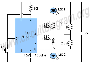
The schematic shown below is a 555 timer circuit. The NE555 is a well-known integrated circuit that comes in an 8-pin dual in-line package (DIP). There is a vast array of circuits utilizing the 555 IC, which contributes to...
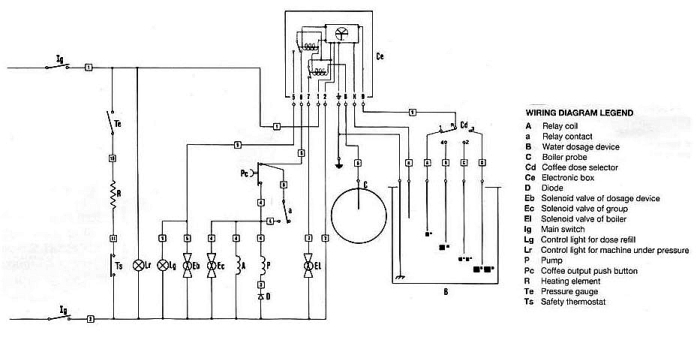
The pump is designed to stop only when the volume set by the four-position selector switch has been reached. However, it will also stop if certain conditions are met. Pressing the brew button (`Pc`) momentarily closes the circuit, sending...
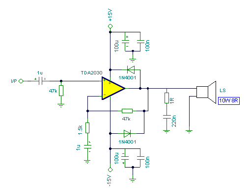
Connecting two TDA2030 through inexpensive power transistors allows for the creation of an amplifier capable of delivering higher power. This can be achieved by utilizing the component values specified in the schematic. To implement this circuit, two TDA2030 integrated circuits...