
Micropower Low Noise Boost Converters with Output Disconnect
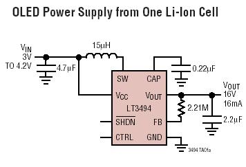
The LT3494 and LT3494A are designed as highly efficient boost converters, suitable for various applications where low noise and compact size are critical. The integration of a power switch and Schottky diode within a single package enhances the overall efficiency and reduces the number of external components required, simplifying circuit design. The innovative control technique employed in these converters minimizes output voltage ripple, which is essential in sensitive electronic applications, such as RF systems, audio devices, and precision instrumentation.
The quiescent current specification of 65 µA indicates that the LT3494 and LT3494A are well-suited for battery-powered applications, where power conservation is necessary. The ability to reduce this current to less than 1 µA during shutdown makes these devices particularly advantageous for portable devices that require long battery life.
The CTRL pin feature allows designers to customize the output voltage to meet specific application requirements, enhancing the versatility of the LT3494 and LT3494A. This capability is particularly useful in applications where the output voltage needs to be adjusted dynamically based on varying load conditions or system requirements.
The compact DFN package (3mm x 2mm) of the LT3494 and LT3494A is conducive to space-constrained designs, allowing for more efficient use of PCB real estate. This small footprint, combined with the integrated components, makes these boost converters ideal for modern electronic devices where size and efficiency are paramount.
Overall, the LT3494 and LT3494A are robust solutions for engineers looking to implement reliable and efficient boost conversion in their designs, with the added benefit of comprehensive support through demo boards and technical assistance from Linear Technology.The LT3494/LT3494A are low noise boost converters with integrated power switch, Schottky diode and output disconnect circuitry. The parts use a novel* control technique resulting in low output voltage ripple as well as high ef ¬ciency over a wide load current range.
This technique guarantees that the switching frequency stays above the audio band for the entire load range. The parts feature a high performance NPN power switch with a 350mA and 180mA current limit for the LT3494A and LT3494 respectively. The quiescent current is a low 65 µA, which is further reduced to less than 1 µA in shutdown. The internal disconnect circuitry allows the output voltage to be isolated from the input during shutdown.
An auxiliary reference input (CTRL pin) overrides the internal 1. 225V feedback reference with any lower value allowing full control of the output voltage during operation. The LT3494/LT3494A are available in a tiny 8-lead 3mm x 2mm DFN package. * The USA list pricing shown is for BUDGETARY USE ONLY, shown in United States dollars (FOB USA per unit for the stated volume), and is subject to change.
International prices may differ due to local duties, taxes, fees and exchange rates. For volume-specific price or delivery quotes, please contact your local Linear Technology sales office or authorized distributor. Linear Technology offers many demo boards free of charge to qualified customers. Contact your local sales office or distributor to inquire about a demo board. Certain demo boards are also available for sale via credit card on this website. Demo boards are for evaluation purposes only. It remains the customer`s responsibility to verify proper and reliable operation in the actual end application.
🔗 External reference
Related Circuits
To achieve an optimal voltage swing, the resistance value of R1 must be selected with precision. The sensor resistance, Rsensor, equals a when there is no light exposure and b when light is present. The voltage difference between these...
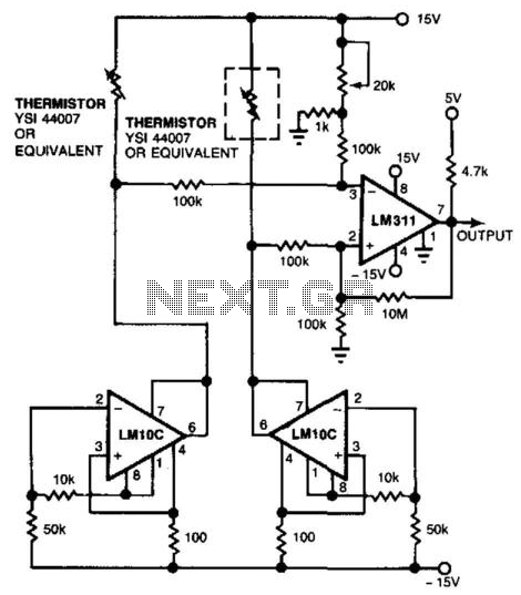
Using a thermistor-bridge circuit, it is possible to detect air losses in system cooling caused by filter or inlet blockage or fan failure. One thermistor is placed directly in the airflow, while the other is shielded. The exposed thermistor...
The signal from a microphone is too weak for a standard line input. This low-noise DC-coupled microphone amplifier provides a solution for anyone who wants to connect a microphone to a high-fidelity installation. As illustrated in the schematic diagram,...
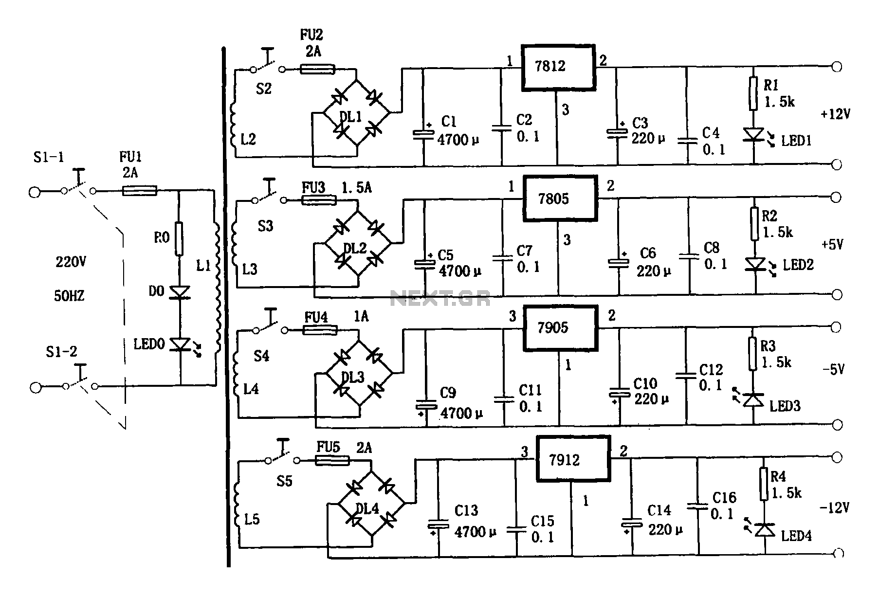
This document presents a multi-output power supply circuit. The circuit utilizes the secondary winding of a transformer and incorporates four voltage regulators: 7812, 7805, 7905, and 7912, providing independent output voltages of +12V, +5V, -5V, and -12V, respectively. Each...
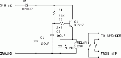
This is a minimal circuit designed for individual audio amplifier projects to control the presenter output relay. The purpose of this circuit is to manage the relay that activates the speaker output within the audio amplifier. The circuit introduces...
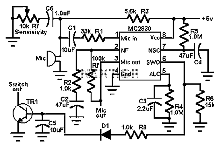
The circuit schematic utilizes the MC2830 voice circuit. Traditional voice circuits are unable to differentiate between speech and noise in the input signal. In noisy environments, such as those caused by switches, this limitation is significant. To address this...